Analog Electronics
BJT
Small signal analysis of BJT
Questions mapped to Small signal analysis of BJT under BJT.
7
Total0
Attempted0
Correct0
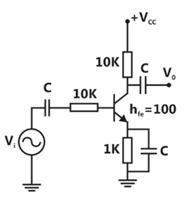
IncorrectThe magnitude of the mid – band voltage gain of the circuit shown in figure is (assuming of the transistor to be 100)

Sign in to see the solution
Log in to view the explanation, track your attempts, and keep your progress.
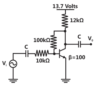
Sign in to UnlockThe voltage gain of the circuit shown below is





Sign in to see the solution
Log in to view the explanation, track your attempts, and keep your progress.
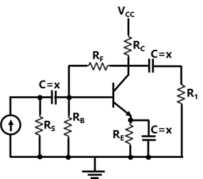
Sign in to UnlockThe feedback used in the circuit shown in figure can be classified as
Sign in to see the solution
Log in to view the explanation, track your attempts, and keep your progress.
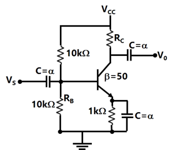
Sign in to UnlockThe trans-conductance of the transistor shown in figure is 10mS. The value of the input resistance is






Sign in to see the solution
Log in to view the explanation, track your attempts, and keep your progress.
Sign in to UnlockThe transistor in the amplifier circuit shown in figure is biased at . Use


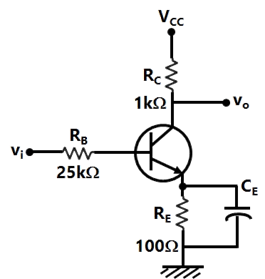
AC small signal mid-band voltage gain = -6.623
AC small signal mid-band voltage gain = -5.565
Value of for the circuit to have a lower cutoff

frequency of 10 Hz = 265.08 micro F
Value of for the circuit to have a lower cutoff
frequency of 10 Hz = 365.08 micro F
Sign in to see the solution
Log in to view the explanation, track your attempts, and keep your progress.
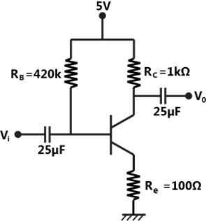
Sign in to UnlockFor the small signal BJT amplifier shown in fig, Assume β = 100 and Frequency =1 kHz
Sign in to see the solution
Log in to view the explanation, track your attempts, and keep your progress.
Sign in to UnlockFigure shows a common emitter amplifier
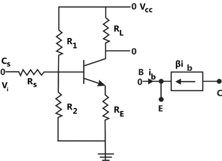
(a) Simplify the circuit by applying Thevenin’s theorem to the biasing network at the base of the transistor

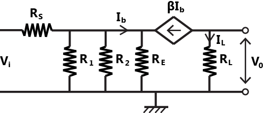
(b) Assuming to be a short for the frequency range considered. Draw the small signal a.c. model of the circuit obtained in (a) by using the simple model for the transistor shown in figure.

(c) Evaluate the small signal gain of the amplifier.

Small signal a.c. model



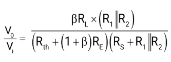
Sign in to see the solution
Log in to view the explanation, track your attempts, and keep your progress.
Sign in to Unlock