Digital Electronics
Sequential Circuits
Practice questions from Sequential Circuits.
36
Total0
Attempted0
Correct0
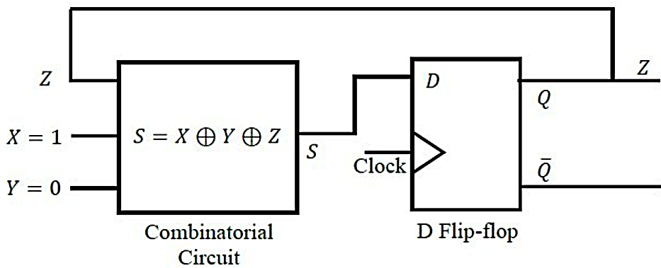
IncorrectIn the circuit, the present value of is 1. Neglecting the delay in the combinatorial circuit, the values of and , respectively, after the application of the clock will be


Sign in to see the solution
Log in to view the explanation, track your attempts, and keep your progress.
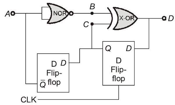
Sign in to UnlockNeglecting the delays due to the logic gates in the circuit shown in figure, the decimal equivalent of the binary sequence of initial logic states, which will not change with clock, is

Sign in to see the solution
Log in to view the explanation, track your attempts, and keep your progress.
Sign in to UnlockA MOD 2 and a MOD 5 up-counter when cascaded together results in a MOD ______ counter. (in integer)
Sign in to see the solution
Log in to view the explanation, track your attempts, and keep your progress.
Sign in to UnlockThe maximum clock frequency in MHz of a 4-stage ripple counter, utilizing flipflops, with each flip-flop having a propagation delay of 20 ns, is ___________. (round off to one decimal place)
Sign in to see the solution
Log in to view the explanation, track your attempts, and keep your progress.
Sign in to UnlockA 16-bit synchronous binary up-counter is clocked with a frequency fCLK. The two most significant bits are OR-ed together to form an output Y. Measurements show' that Y is periodic, and the duration for which Y remains high in each period is 24 ms. The clock frequency fCLK is _________ MHz. (Round off to 2 decimal places.)
Sign in to see the solution
Log in to view the explanation, track your attempts, and keep your progress.
Sign in to UnlockA counter is constructed with three D flip-flops. The input-output pairs are named (D0, Q0), (D1, Q1), and (D2, Q2), where the subscript 0 denotes the least significant bit. The output sequence is desired to be the Gray-code sequence 000, 001, 011, 010, 110, 111, 101, and 100, repeating periodically. Note that the bits are listed in the Q2 Q1 Q0 format. The combinational logic expression for D1 is
Q2Q1Q0



Sign in to see the solution
Log in to view the explanation, track your attempts, and keep your progress.
Sign in to UnlockA sequence detector is designed to detect precisely 3 digital inputs, with overlapping sequences detectable. For the sequence (1,0,1) and input data (1,1,0,1,0,0,1,1,0,1,0,1,1,0), what is the output of this detector?
Sign in to see the solution
Log in to view the explanation, track your attempts, and keep your progress.
Sign in to UnlockWhich one of the following statements is true about the digital circuit shown in the figure?

Sign in to see the solution
Log in to view the explanation, track your attempts, and keep your progress.
Sign in to UnlockFor the synchronous sequential circuit shown below, the output Z is zero for the initial conditions

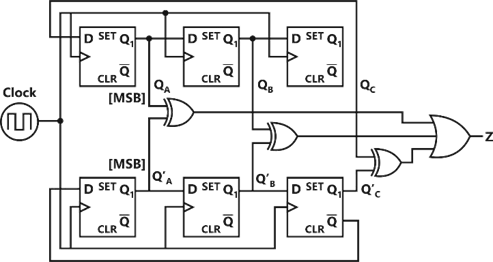
The minimum number of clock cycles after which the output Z would again become zero is ___________.
Sign in to see the solution
Log in to view the explanation, track your attempts, and keep your progress.
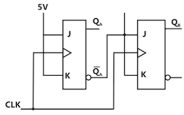
Sign in to UnlockThe current state of a two JK flip-flop system is 00. Assume that the clock rise-time is much smaller than the delay of the JK flip-flop. The next state of the system is

Sign in to see the solution
Log in to view the explanation, track your attempts, and keep your progress.
Sign in to UnlockThe figure shows a digital circuit constructed using negative edge triggered J – K flip flops. Assume a starting state of . This state will repeat after __________ number cycles of the clock CLK.

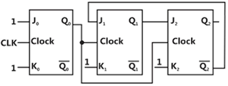
Sign in to see the solution
Log in to view the explanation, track your attempts, and keep your progress.
Sign in to UnlockIn the following sequential circuit, the initial state (before the first clock pulse) of the circuit is . The state , immediately after the 333rd clock pulse is


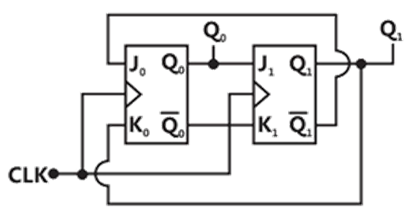
Sign in to see the solution
Log in to view the explanation, track your attempts, and keep your progress.
Sign in to UnlockA cascade of three identical modulo – 5 counters has an overall module of
Sign in to see the solution
Log in to view the explanation, track your attempts, and keep your progress.
Sign in to UnlockWhich of the following is an invalid state in an 8-4-2-1 Binary coded decimal counter
Sign in to see the solution
Log in to view the explanation, track your attempts, and keep your progress.
Sign in to UnlockA JK flip flop can be implemented by T flip-flops. Identify the correct implementation.
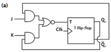
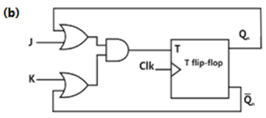
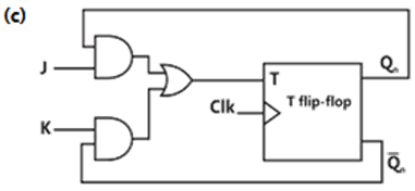
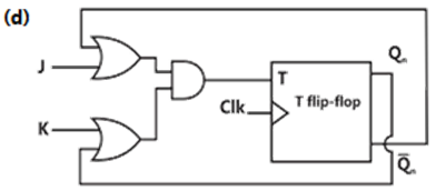
Sign in to see the solution
Log in to view the explanation, track your attempts, and keep your progress.
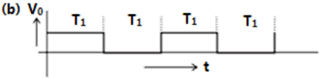
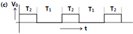
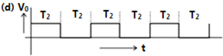
Sign in to UnlockTwo monoshot multivibrators, one positive edge triggered and another negative edge triggered are connected as shown in figure


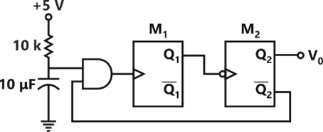
The monoshots and when triggered produce pulse of width and respectively. Where . The steady state output voltage of the circuit is






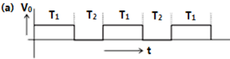
Sign in to see the solution
Log in to view the explanation, track your attempts, and keep your progress.
Sign in to UnlockA 3-bit gray counter is used to control the output of the multiplexer as shown in the figure. The initial state of the counter is . The output is pulled high. The output of the circuit follows the sequence

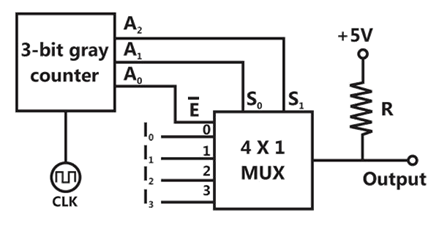




Sign in to see the solution
Log in to view the explanation, track your attempts, and keep your progress.
Sign in to UnlockThe clock frequency applied to the digital circuit shown in the figure below is 1 kHz. If the initial state of the output Q of the flip-flop is 0, then the frequency of the output waveform Q in kHz is
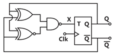
Sign in to see the solution
Log in to view the explanation, track your attempts, and keep your progress.
Sign in to UnlockConsider the given circuit,
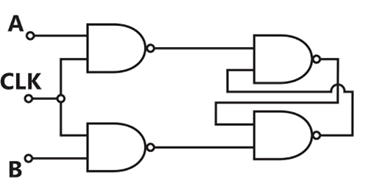
In this circuit, the race around
Sign in to see the solution
Log in to view the explanation, track your attempts, and keep your progress.
Sign in to UnlockThe state transition diagram for the logic circuit shown is
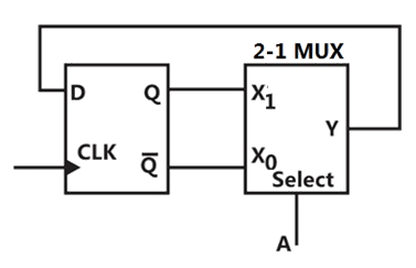
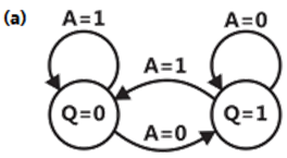
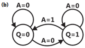
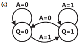
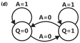
Sign in to see the solution
Log in to view the explanation, track your attempts, and keep your progress.
Sign in to Unlocktwo-bit counter circuit is shown below.
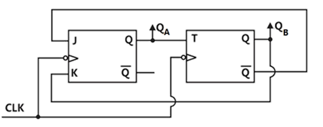
If the state of the counter at the clock time is “10” then the state of the counter at (after three clock cycles) will be



Sign in to see the solution
Log in to view the explanation, track your attempts, and keep your progress.
Sign in to UnlockThe truth table of a monoshot shown in the figure is given in the table below:
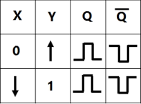
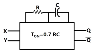
Two monoshots, one positive edge triggered and other negative edge triggered, are connected as shown in the figure. The pulse widths of the two monoshot outputs, , and , are and , respectively.




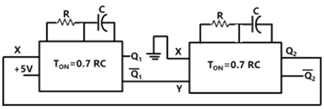
The frequency and the duty cycle of the signal at Q1 will respectively be




Sign in to see the solution
Log in to view the explanation, track your attempts, and keep your progress.
Sign in to UnlockThe digital circuit shown in figure works as a
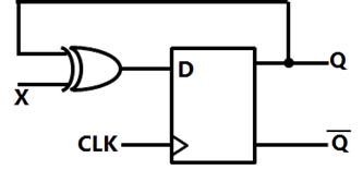
Sign in to see the solution
Log in to view the explanation, track your attempts, and keep your progress.
Sign in to UnlockSelect the circuit, which will produce the given output Q for the input signals X1 and X2 given in Figure.
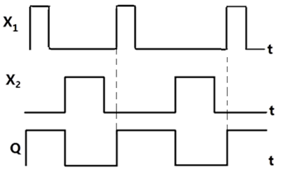
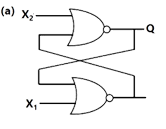
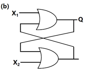
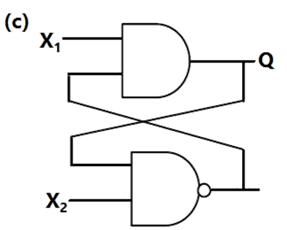
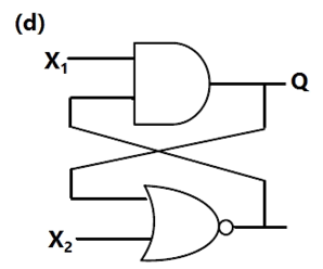
Sign in to see the solution
Log in to view the explanation, track your attempts, and keep your progress.
Sign in to UnlockIn figure, as long as and , the output Q remains


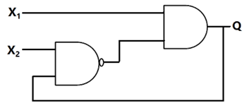
Sign in to see the solution
Log in to view the explanation, track your attempts, and keep your progress.
Sign in to UnlockThe digital circuit shown in figure generates a modified clock pulse at the output. Choose the correct output waveform form the options given below.

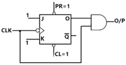
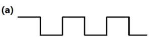



Sign in to see the solution
Log in to view the explanation, track your attempts, and keep your progress.
Sign in to UnlockThe shift register shown in Figure is initially loaded with the bit pattern 1010. Subsequently the shift register is clocked, and with each clock pulse the pattern gets shifted by one bit position to the right. With each shift, the bit at the serial input is pushed to the left most position (MSB). After how many clock pulses will the content of the shift register become 1010 again?
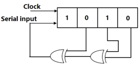
Sign in to see the solution
Log in to view the explanation, track your attempts, and keep your progress.
Sign in to UnlockAn X-Y flip flop, whose Characteristic Table is given below is to be implemented using a J-K flip flop

This can be done by making




Sign in to see the solution
Log in to view the explanation, track your attempts, and keep your progress.
Sign in to UnlockThe frequency of the clock signal applied to the rising edge triggered D flip-flop shown in figure is 10 kHz. The frequency of the signal available at Q is
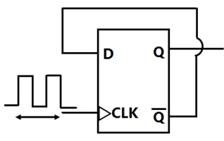
Sign in to see the solution
Log in to view the explanation, track your attempts, and keep your progress.
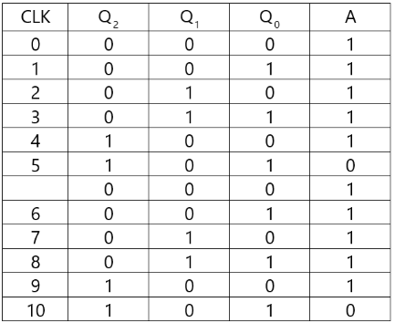
Sign in to UnlockThe ripple counter shown in figure is made up negative edge triggered J-K flips flops. The signal levels at J and K inputs of all the flip-flops are maintained at logic 1. Assume that all outputs are cleared just prior to applying the clock signal.

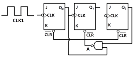
(a) Create a table of Q0, Q1, Q2 and A in the format given below for 10 successive input cycles of the clock CLK1.
(b) Determine the module number of the counter.
(c) Modify the circuit of given figure to create a module-6 counter using the same components used in the figure.
(a)
(b) Mod-8 counter
(c) The NAND gate input should be changed to instead of .
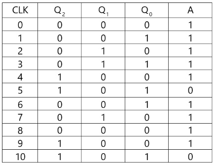


i.e. A

(a)
(b) Mod-6 counter
(c) The NAND gate input should be changed to instead of .
i.e. A
(a)
(b) Mod-5 counter
(c) The NAND gate input should be changed to instead of .
i.e. A
None
Sign in to see the solution
Log in to view the explanation, track your attempts, and keep your progress.
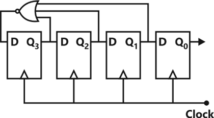
Sign in to UnlockFor the ring counter shown in figure, find the steady state sequence if the initial state of the counters is 1110 (i.e., Q3, Q2, Q1, Q0 = 1110). Determine the MOD number of the counter.
Sign in to see the solution
Log in to view the explanation, track your attempts, and keep your progress.
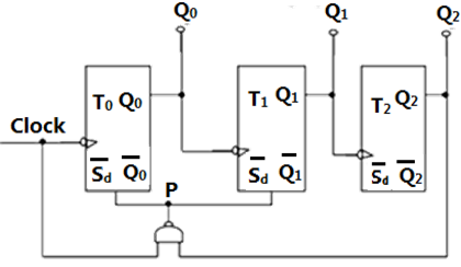
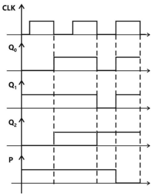
Sign in to UnlockThe counter shown in the figure, is initially in state . With reference to the CLK input, draw waveforms for and P for the next three CLK cycles.


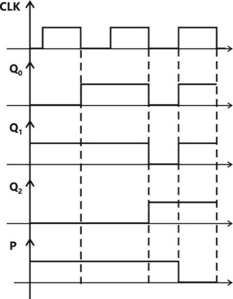
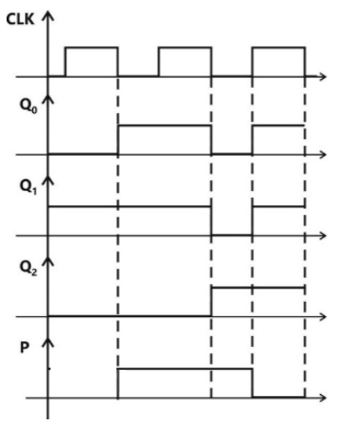
None
Sign in to see the solution
Log in to view the explanation, track your attempts, and keep your progress.
Sign in to UnlockFor a flip-flop formed from two NAND gates as shown, the unusable state corresponds to
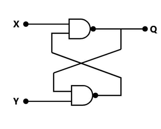
Sign in to see the solution
Log in to view the explanation, track your attempts, and keep your progress.
Sign in to Unlock
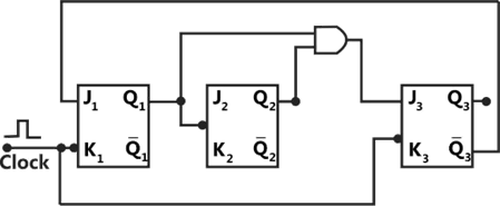
(a) Construct the truth table for the circuit given. are outputs and the clock pulses are the inputs. Unused J, K inputs are assumed to be at logic 1. All flip-flops are rest at power ON.

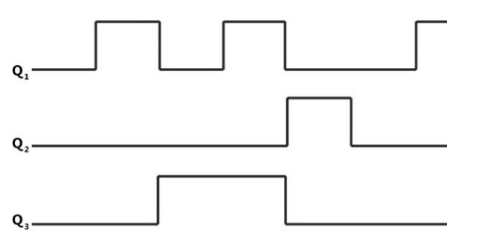
(b) Sketch the output waveforms at
(c) What function does this circuit perform?
(a)
(b)
(c) MOD-5 counter
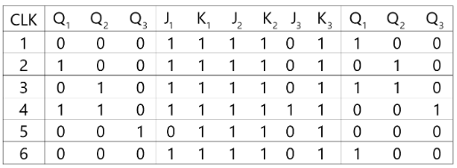
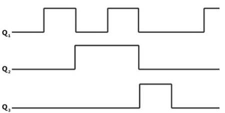
(a)
(b)
(c) MOD-6 counter
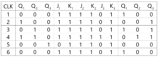
(a)
(b)
(c) MOD-4 counter
None
Sign in to see the solution
Log in to view the explanation, track your attempts, and keep your progress.
Sign in to UnlockFor a J-K flip-flop its J input is tied to its own output and its K input is connected to its own Q output. If the flip-flop is fed with a clock of frequency 1MHz, its Q output frequency will be _________________

Sign in to see the solution
Log in to view the explanation, track your attempts, and keep your progress.
Sign in to UnlockThe three stage Johnson ring counter shown in figure is clock at a constant frequency of from the starting stage of . The frequency of outputs will be



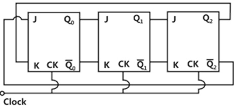




Sign in to see the solution
Log in to view the explanation, track your attempts, and keep your progress.
Sign in to Unlock