Digital Electronics
Logic Family
Practice questions from Logic Family.
10
Total0
Attempted0
Correct0
IncorrectThe MOSFET switches shown in the circuit are ideal.
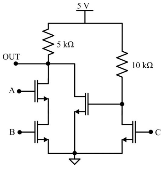
Which of the following is the correct option for Boolean logical expression of the output (OUT), and the maximum possible power (P) consumed by the circuit?
OUT

OUT


Sign in to see the solution
Log in to view the explanation, track your attempts, and keep your progress.
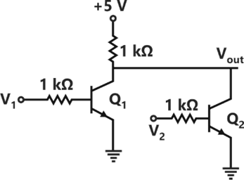
Sign in to UnlockThe logical gate implemented using the circuit shown below where, V1 and V2 are inputs (with 0 V as digital 0 and 5 V as digital 1) and VOUT is the output, is
Sign in to see the solution
Log in to view the explanation, track your attempts, and keep your progress.
Sign in to UnlockA hysteresis type TTL inverter is used to realize an oscillator in the circuit shown in the figure.
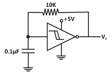
If the lower and upper trigger level voltages are 0.9V and 1.7V, the period (in ms), for which output is LOW, is ______________.
Sign in to see the solution
Log in to view the explanation, track your attempts, and keep your progress.
Sign in to UnlockIn the circuit shown below, Q1 has negligible collector-to-emitter saturation voltage and the diode drops negligible voltage across it under forward bias. If Vcc. is +5 V, X and Y are digital signals with 0 V as logic 0 and Vcc. as logic 1, then the Boolean expression for Z is
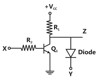
X Y


Sign in to see the solution
Log in to view the explanation, track your attempts, and keep your progress.
Sign in to UnlockThe increasing order of speed of data access for the following devices is
(i) Cache Memory
(ii) CDROM
(iii) Dynamic RAM
(iv) Processor Registers
(v) Magnetic Tape
Sign in to see the solution
Log in to view the explanation, track your attempts, and keep your progress.
Sign in to UnlockA TTL NOT gate circuit is shown in figure. Assuming VBE = 0.7V of both the transistors, if Vi = 3.0 V, then the states of the two transistors will be
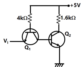
ON and OFF


reverse ON and OFF
reverse ON and ON
OFF and reverse ON
Sign in to see the solution
Log in to view the explanation, track your attempts, and keep your progress.
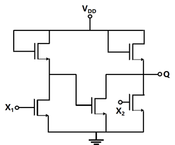
Sign in to UnlockIf X1 and X2 are the inputs to the circuit shown in figure, the output Q is:


Sign in to see the solution
Log in to view the explanation, track your attempts, and keep your progress.
Sign in to UnlockThe digital circuit using two inverters shown in figure will act as

Sign in to see the solution
Log in to view the explanation, track your attempts, and keep your progress.
Sign in to UnlockThe open collector outputs of two 2-inputs NAND gates are connected to a common pull up resistor. If the input to the gates are P, Q and R, S respectively, the output is equal to


Sign in to see the solution
Log in to view the explanation, track your attempts, and keep your progress.
Sign in to UnlockIn standard TTL gates, the totem pole output stage is primarily used to
Sign in to see the solution
Log in to view the explanation, track your attempts, and keep your progress.
Sign in to Unlock