Power Electronics
Power Semiconductor Devices
Practice questions from Power Semiconductor Devices.
49
Total0
Attempted0
Correct0
IncorrectThe figure shows a straight-line approximation for the forward characteristics of a power diode. A continuous on-state current of 15 A is flowing through the diode.
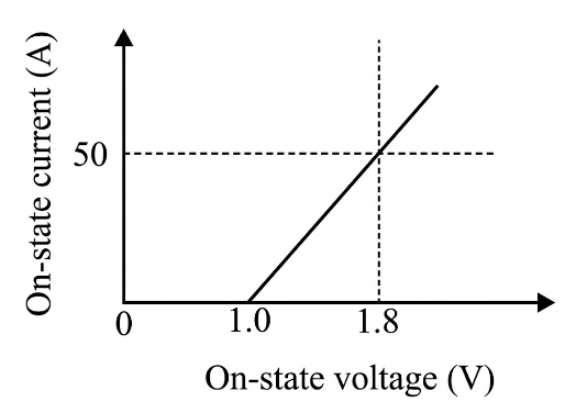
What is the power loss in the diode?
Sign in to see the solution
Log in to view the explanation, track your attempts, and keep your progress.
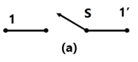
Sign in to UnlockConsider the circuit shown in Figure (a). A gate pulse is applied between time instants and . After , during the MOSFET turn OFF process, it experiences a voltage overshoot.


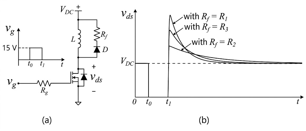
Based on the waveforms shown in Figure (b), which one of the following options is correct?


Sign in to see the solution
Log in to view the explanation, track your attempts, and keep your progress.
Sign in to UnlockIf the following switching devices have similar power ratings, which one of them is the fastest?
Sign in to see the solution
Log in to view the explanation, track your attempts, and keep your progress.
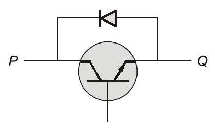
Sign in to UnlockA semiconductor switch needs to block voltage of only one polarity during OFF state as shown in figure (i) and carry current in both directions during ON state as shown in figure (ii). Which of the following switch combination(s) will realize the same?


Fig. (i)
Fig. (ii)
Sign in to see the solution
Log in to view the explanation, track your attempts, and keep your progress.
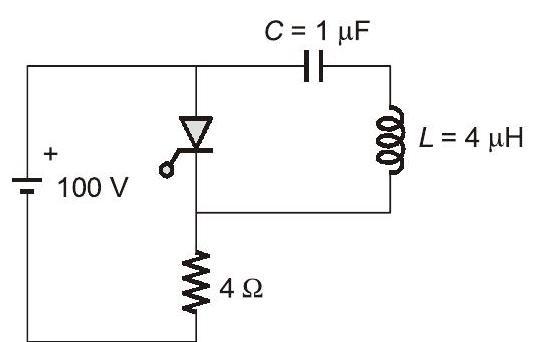
Sign in to UnlockThe circuit shown in the figure has reached steady state with thyristor '' in OFF condition. Assume that the latching and holding currents of the thyristor are zero. The thyristor is turned at . The duration in microseconds for which the thyristor would conduct, before it turns off, is ___ (Round off to 2 decimal places).


Sign in to see the solution
Log in to view the explanation, track your attempts, and keep your progress.
Sign in to UnlockA charger supplies 100 W at 20 V for charging the battery of a laptop. The power devices, used in the converter inside the charger, operate at a switching frequency of 200 kHz. Which power device is best suited for this purpose?
Sign in to see the solution
Log in to view the explanation, track your attempts, and keep your progress.
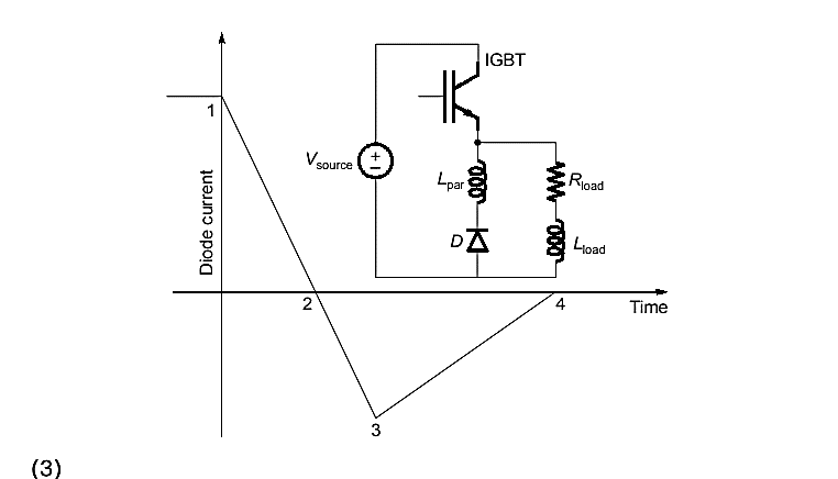
Sign in to UnlockA double pulse measurement for an inductively loaded circuit controlled by the IGBT switch is carried out to evaluate the reverse recovery characteristics of the diode. D, represented approximately as a piecewise linear plot of current vs time at diode turn-off. is a parasitic inductance due to the wiring of the circuit, and is in series with the diode. The point on the plot (indicate your choice by entering 1, 2, 3 or 4) at which the IGBT experiences the highest current stress is

Sign in to see the solution
Log in to view the explanation, track your attempts, and keep your progress.
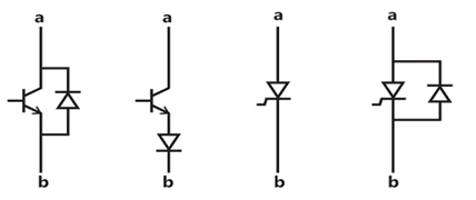
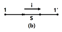
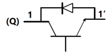
Sign in to UnlockFour power semiconductor devices are shown in the figure along with their relevant terminals. The device(s) that can carry dc current continuously in the direction shown when gated appropriately is (are)

Sign in to see the solution
Log in to view the explanation, track your attempts, and keep your progress.
Sign in to UnlockFor the power semiconductor devices IGBT, MOSFET, Diode and Thyristor, which one of the following statements is TRUE?
Sign in to see the solution
Log in to view the explanation, track your attempts, and keep your progress.
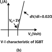
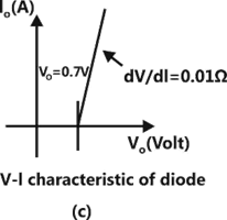
Sign in to UnlockA steady dc current of 100A is flowing through a power module (S, D) as shown in Figure (a). The V-I characteristics of the IGBT (S) and the diode (D) are shown in the Figure (b) and (c), respectively. The conduction power loss in the power module (S, D), in watts, is ________________.

Sign in to see the solution
Log in to view the explanation, track your attempts, and keep your progress.
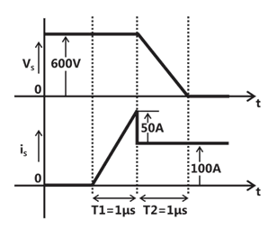
Sign in to UnlockThe voltage across and the current through a semiconductor switch during a turn-ON transition are shown in figure. The energy dissipated during the turn-ON transition, in mJ, is ____________.


Sign in to see the solution
Log in to view the explanation, track your attempts, and keep your progress.
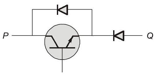
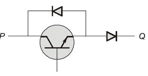
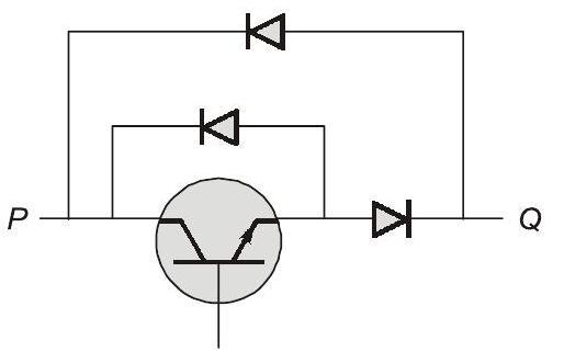
Sign in to UnlockFigure shows four electronic switches (i), (ii), (iii) and (iv). Which of the switches can block voltages of either polarity (applied between terminals ‘a’ and ‘b’) when the active device is in the OFF state?
(i) (ii) (iii) (iv)
Sign in to see the solution
Log in to view the explanation, track your attempts, and keep your progress.
Sign in to UnlockThe SCR in the circuit shown has a latching current of 40mA. A gate pulse of 50 μs is applied to the SCR. The maximum value of R in to ensure successful firing of the SCR is ___________.

Sign in to see the solution
Log in to view the explanation, track your attempts, and keep your progress.
Sign in to UnlockThe typical ratio of latching current to holding current in a 20A thyristor is
Sign in to see the solution
Log in to view the explanation, track your attempts, and keep your progress.
Sign in to UnlockCircuit turn-off time of an SCR is defined as the time
Sign in to see the solution
Log in to view the explanation, track your attempts, and keep your progress.
Sign in to UnlockFigure shows a composite switch consisting of a power transistor (BJT) in series with a diode. Assuming that the transistor switch and the diode are ideal, the I-V characteristics of the composite switch is
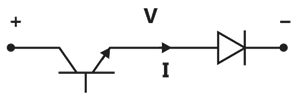
Sign in to see the solution
Log in to view the explanation, track your attempts, and keep your progress.
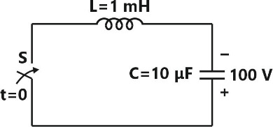
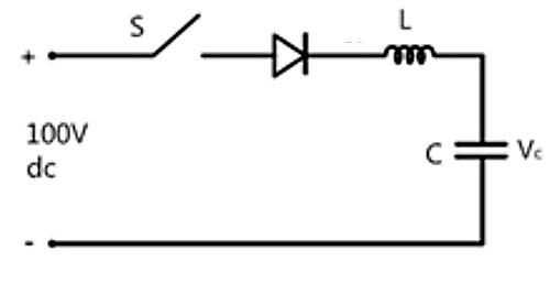
Sign in to UnlockThe L-C circuit shown in the figure has an impedance L = I mH and a capacitance C = 10uF.
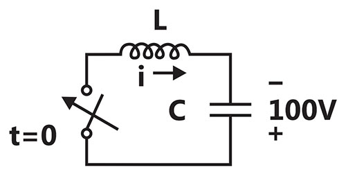
The initial current through the inductor is zero, while the initial capacitor voltage is 100V. The switch is closed at t = 0. The current i through the circuit is:


Sign in to see the solution
Log in to view the explanation, track your attempts, and keep your progress.
Sign in to UnlockThe L-C circuit shown in the figure has an impedance L = I mH and a capacitance C = 10uF.
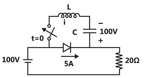
The LC circuit shown in the figure has an inductance and capacitance . The LC circuit is used to commutate a thyristor, which is initially carrying a current of 5A as shown in the figure below. The values and initial of and are same as in previous question. The switch is closed ae . If the forward drop is negligible, the time taken for the device to turn off is


Sign in to see the solution
Log in to view the explanation, track your attempts, and keep your progress.
Sign in to UnlockAn SCR is considered to be a semi-controlled device because
Sign in to see the solution
Log in to view the explanation, track your attempts, and keep your progress.
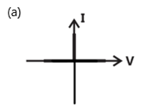
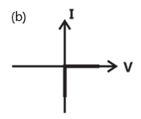
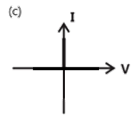
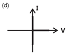
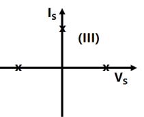
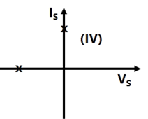
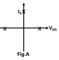
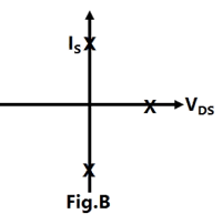
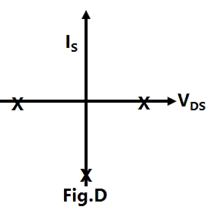
Sign in to UnlockMatch the switch arrangements on the top row to the steady-state V-I characteristics on the lower row. The steady state operating points are shown by large black dots.


Sign in to see the solution
Log in to view the explanation, track your attempts, and keep your progress.
Sign in to UnlockThe circuit in the figure is a current commutated dc-dc chopper where. is the main SCR and is the auxiliary SCR. The load current is constant at 10A. is ON. is triggered at t = 0. is turned OFF between


Sign in to see the solution
Log in to view the explanation, track your attempts, and keep your progress.
Sign in to UnlockA 1:1 Pulse Transformer (PT) is used to trigger the SCR in the adjacent figure. The SCR is rated at 1.5 kV,250A with 250mA, 150mA, and 150mA, 100mA. The SCR is connected to an inductive load, where L = 150mH in series with a small resistance and the supply voltage is 200V dc. The forward drops of all transistors/diodes and gate-cathode junction during ON state are 1.0 V


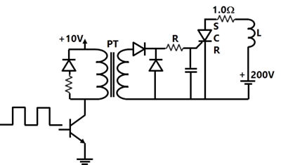
The resistance R should be
Sign in to see the solution
Log in to view the explanation, track your attempts, and keep your progress.
Sign in to UnlockA 1:1 Pulse Transformer (PT) is used to trigger the SCR in the adjacent figure. The SCR is rated at 1.5 kV,250A with 250mA, 150mA, and 150mA, 100mA. The SCR is connected to an inductive load, where L = 150mH in series with a small resistance and the supply voltage is 200V dc. The forward drops of all transistors/diodes and gate-cathode junction during ON state are 1.0 V
The minimum approximate volt-second rating of the pulse transformer suitable for triggering the SCR should be: (volt-second rating is the maximum of product of the voltage and the width of the pulse that may be applied)
Sign in to see the solution
Log in to view the explanation, track your attempts, and keep your progress.
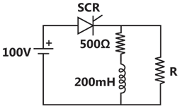
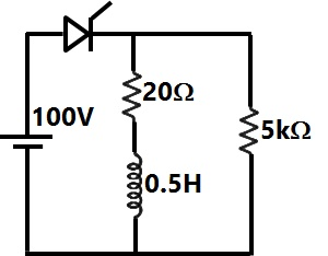
Sign in to UnlockA voltage commutation circuit is shown in figure. If the turn off time of the SCRs is 50µ sec and a safety margin of 2 is considered, then what will be the approximate minimum value of capacitor required for proper commutation?

Sign in to see the solution
Log in to view the explanation, track your attempts, and keep your progress.
Sign in to UnlockAn SCR having a turn ON time of 5µsec, latching current of 50mA and holding current of 40mA is triggered by a short duration pulse and is used in the circuit shown in figure. The minimum pulse width required to turn the SCR ON will be
Sign in to see the solution
Log in to view the explanation, track your attempts, and keep your progress.
Sign in to UnlockThe conduction loss versus device current characteristic of a power MOSFET is best approximated by
Sign in to see the solution
Log in to view the explanation, track your attempts, and keep your progress.
Sign in to UnlockFigure shows the voltage across a power semiconductor device and the current through the device during a switching transition. Is the transition a turn ON transition or a turn OFF transition? What is the energy lost during the transition?
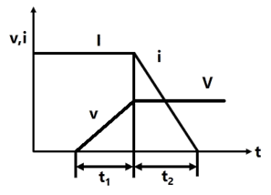
Turn ON,

Turn OFF,

Turn ON,
Turn OFF,
Sign in to see the solution
Log in to view the explanation, track your attempts, and keep your progress.
Sign in to UnlockAn electronic switch S is required to block voltages of either polarity during its OFF state as shown in Figure a. This switch is required to conduct in only one direction during its ON state as shown in Figure b.
Which of the following are valid realizations of the switch S?


Sign in to see the solution
Log in to view the explanation, track your attempts, and keep your progress.
Sign in to UnlockThe triggering circuit of a thyristor is shown in figure. The thyristor requires a gate current of 10 mA, for guaranteed turn-on. The value of R required for the thyristor to turn on reliably under all conditions of variation is

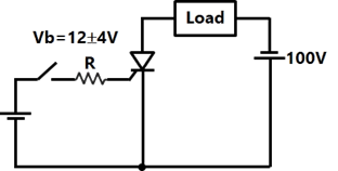
Sign in to see the solution
Log in to view the explanation, track your attempts, and keep your progress.
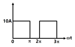
Sign in to UnlockA MOSFET rated for 15 A, carries a periodic current as shown in figure. The ON state resistance of the MOSFET is 0.15Ω. The average ON state loss in the MOSFET is
Sign in to see the solution
Log in to view the explanation, track your attempts, and keep your progress.
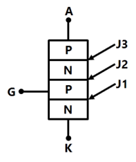
Sign in to UnlockFigure shows a thyristor with the standard terminations of anode (A), cathode (K), gate (G) and the different junctions named J1, J2 and J3. When the thyristor is turned on and conducting
Sign in to see the solution
Log in to view the explanation, track your attempts, and keep your progress.
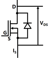
Sign in to UnlockFigure shown a MOSFET with an integral body diode. It is employed as a power switching device in the ON and OFF states through appropriate control. The ON and OFF states of the switch are given on the plane by


Sign in to see the solution
Log in to view the explanation, track your attempts, and keep your progress.
Sign in to UnlockThe main reason for connecting a pulse transformer at the output stage of a thyristor triggering circuit is to
Sign in to see the solution
Log in to view the explanation, track your attempts, and keep your progress.
Sign in to UnlockFor perfectly balanced operation a certain three phase ac power electronic circuit generates odd harmonic currents of order five and seven in the three phases of the ac mains. Identify which of these harmonics form a positive-sequence system, and which form a negative – sequence system.
Sign in to see the solution
Log in to view the explanation, track your attempts, and keep your progress.
Sign in to UnlockThe uncontrolled electric switch employed in power electric converters is:
Sign in to see the solution
Log in to view the explanation, track your attempts, and keep your progress.
Sign in to UnlockThe MOSFET switch in its on-state may be considered equivalent to:
Sign in to see the solution
Log in to view the explanation, track your attempts, and keep your progress.
Sign in to UnlockIn a commutation circuit employed to turn off an SCR, satisfactory turn-off is obtained when
Sign in to see the solution
Log in to view the explanation, track your attempts, and keep your progress.
Sign in to UnlockIf a diode is connected in anti-parallel with a thyristor, then
Sign in to see the solution
Log in to view the explanation, track your attempts, and keep your progress.
Sign in to UnlockWhich semiconductor power device out of the following is not a current triggered device?
Sign in to see the solution
Log in to view the explanation, track your attempts, and keep your progress.
Sign in to UnlockThe triac can be used only in
Sign in to see the solution
Log in to view the explanation, track your attempts, and keep your progress.
Sign in to UnlockWhich of the following does not cause permanent damage of an SCR?
Sign in to see the solution
Log in to view the explanation, track your attempts, and keep your progress.
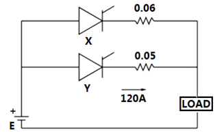
Sign in to UnlockFigure, show two thyristors each rated 500A (continuous) sharing a load current. Current through thyristor Y is 120A. The current through thyristor X will be nearly ______________ A.
Sign in to see the solution
Log in to view the explanation, track your attempts, and keep your progress.
Sign in to UnlockConsider the thyristor circuit of figure. The Thyristor is given a triggering pulse after every 10ms. Calculate the duration for which the thyristor remains ON after each triggering pulse. Assume ideal devices and explain briefly the basis.
Sign in to see the solution
Log in to view the explanation, track your attempts, and keep your progress.
Sign in to UnlockA switched mode power supply operating at 20 kHz to 100 kHz range uses as the main switching element
Sign in to see the solution
Log in to view the explanation, track your attempts, and keep your progress.
Sign in to UnlockA triac can be triggered by a gate pulse of ______________ polarity.
Sign in to see the solution
Log in to view the explanation, track your attempts, and keep your progress.
Sign in to UnlockThe thermal resistance between the body of a power semiconductor device and the ambient is expressed as
Sign in to see the solution
Log in to view the explanation, track your attempts, and keep your progress.
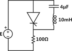
Sign in to UnlockIn the circuit of figure, the switch ‘S’ is closed at t=0 with . In the steady state equals


Sign in to see the solution
Log in to view the explanation, track your attempts, and keep your progress.
Sign in to UnlockThe operating state that distinguishes a silicon controlled rectifier (SCR) from a diode is
Sign in to see the solution
Log in to view the explanation, track your attempts, and keep your progress.
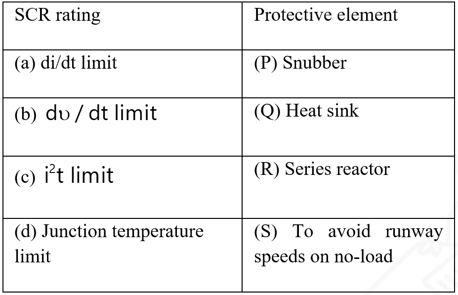
Sign in to UnlockMatch the functions of the following protective elements in SCR applications:
Sign in to see the solution
Log in to view the explanation, track your attempts, and keep your progress.
Sign in to Unlock