Analog Electronics
Diode and Its Applications
Practice questions from Diode and Its Applications.
35
Total0
Attempted0
Correct0
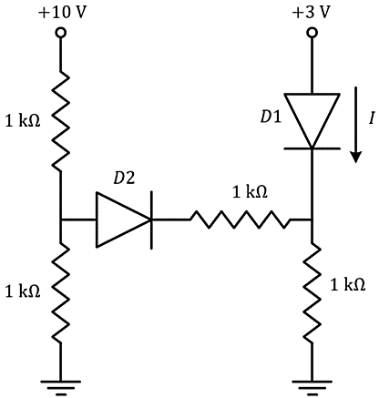
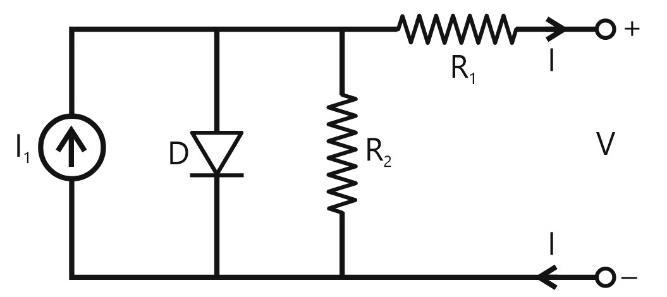
IncorrectIn the given circuit, the diodes are ideal. The current through the diode in milliamperes is ________ (rounded off to two decimal places).


Sign in to see the solution
Log in to view the explanation, track your attempts, and keep your progress.
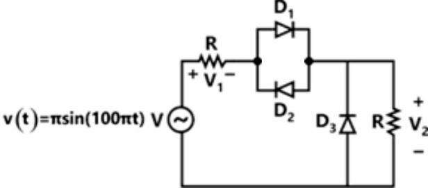
Sign in to UnlockAll the elements in the circuit shown in the following figure are ideal. Which of the following statements is/are true?
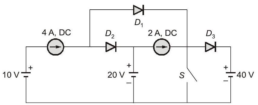
When switch is , both and conducts and is reverse biased.


When switch is conducts and both and are reverse biased.

When switch is OFF, is reverse biased and both and conduct.
When switch is OFF, conducts, is reverse biased and conducts.
Sign in to see the solution
Log in to view the explanation, track your attempts, and keep your progress.
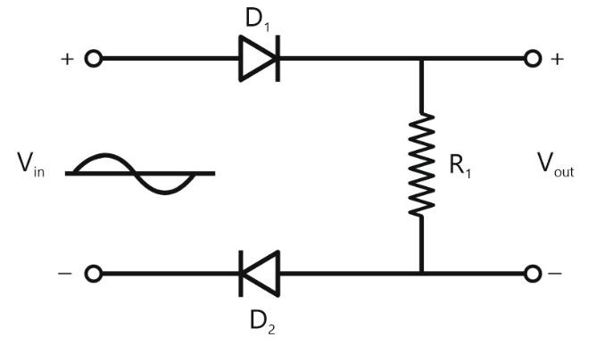
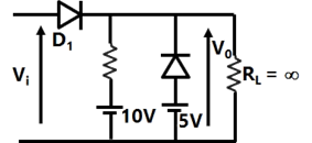
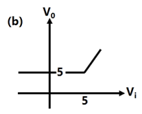
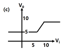
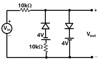
Sign in to UnlockFor the circuit shown below with ideal diodes the output will be


Sign in to see the solution
Log in to view the explanation, track your attempts, and keep your progress.
Sign in to UnlockIn the circuit shown, the input is a sinusoidal AC voltage having an RMS value of 230V±20%. The worst-case peak-inverse voltage seen across any diode is _________ V. (Round off to 2 decimal places.)


Sign in to see the solution
Log in to view the explanation, track your attempts, and keep your progress.
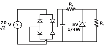
Sign in to UnlockIn the circuit shown, a 5V Zener diode is used to regulate the voltage across load . The input is an unregulated DC voltage with a minimum value of 6V and a maximum value of 8V. The value of is 6Ω. The Zener diode has a maximum rated power dissipation of 2.5 W, Assuming the Zener diode to be ideal, the minimum value of is ___________ Ω.


Sign in to see the solution
Log in to view the explanation, track your attempts, and keep your progress.
Sign in to UnlockThe waveform shown in solid line is obtained by clipping a full-wave rectified sinusoid (shown dashed). The ratio of the RMS value of the full wave rectified waveform to the RMS value of the clipped waveform is _______.
(Round off to 2 decimal places.)

Sign in to see the solution
Log in to view the explanation, track your attempts, and keep your progress.
Sign in to UnlockConsider the diode circuit shown below. The diodes D, obeys the current-voltage characteristic

where n>1, , is the voltage across the diode and is the current through it. The circuit is biased so that voltage, V > 0 and current, I<0, If you had to design this circuit to transfer maximum power from the current source to a resistive load (not shown) at the output, what values and would you choose?


Small and small
Large and large
Small and large
Large and small
Sign in to see the solution
Log in to view the explanation, track your attempts, and keep your progress.
Sign in to UnlockA non-ideal diode is biased with a voltage of –0.03 V, and a diode current of is measured. The thermal voltage is 26 mV and the ideality factor for the diode is 15/13. The voltage, in V, at which the measured current increases to is closest to:


Sign in to see the solution
Log in to view the explanation, track your attempts, and keep your progress.
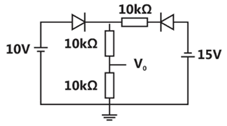
Sign in to UnlockFor the circuit shown in the figure below, assume that diodes are ideal.

The DC components of voltages, respectively are

Sign in to see the solution
Log in to view the explanation, track your attempts, and keep your progress.
Sign in to UnlockIn the following circuit, the input voltage is 100. For , the average voltage across R (in volts) under steady – state is nearest to


Sign in to see the solution
Log in to view the explanation, track your attempts, and keep your progress.
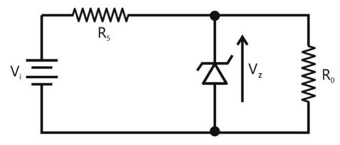
Sign in to UnlockThe sinusoidal ac source in the figure has an RMS value of . Considering all possible values of , the minimum value of in 3 to avoid burnout of the Zener diode is __________.


Sign in to see the solution
Log in to view the explanation, track your attempts, and keep your progress.
Sign in to UnlockAssuming the diodes to be ideal in the figure, for the output to be clipped, the input voltage must be outside the range
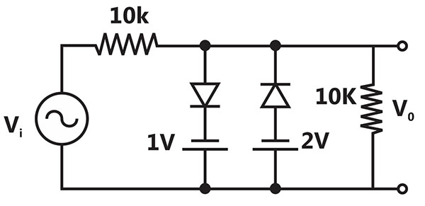
Sign in to see the solution
Log in to view the explanation, track your attempts, and keep your progress.
Sign in to UnlockIn the circuit shown below, the knee current of the ideal Zener diode is 10mA. To maintain 5 V across , in Ω and the minimum power rating of the Zener diode in mW respectively are
Sign in to see the solution
Log in to view the explanation, track your attempts, and keep your progress.
Sign in to UnlockA voltage Volts is applied across YZ. Assuming ideal diodes, the voltage measured across WX in Volts, is

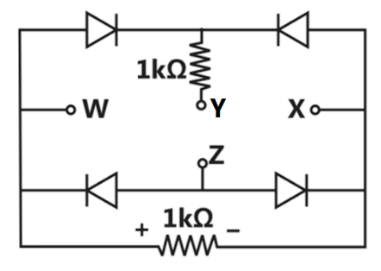


0 for all t
Sign in to see the solution
Log in to view the explanation, track your attempts, and keep your progress.
Sign in to UnlockThe i-v characteristics of the diode in the circuit given below are

The current in the circuit is
Sign in to see the solution
Log in to view the explanation, track your attempts, and keep your progress.
Sign in to UnlockA clipper circuit shown below
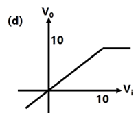
Assuming forward voltage drops of the diodes to be 0.7V, the input-output transfer characteristics of the circuit is
Sign in to see the solution
Log in to view the explanation, track your attempts, and keep your progress.
Sign in to UnlockAssuming that the diodes in the given circuit are ideal, the voltage is

Sign in to see the solution
Log in to view the explanation, track your attempts, and keep your progress.
Sign in to UnlockThe following circuit has a source voltage Vs as shown in the graph. The current through the circuit is also shown.
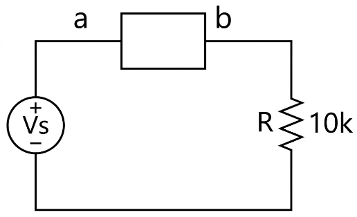
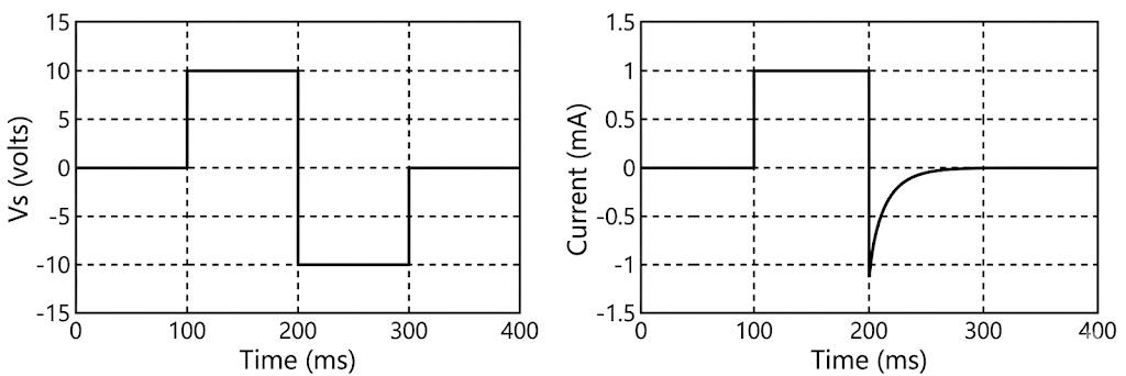
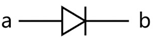
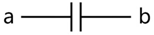
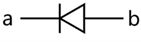
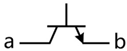
The element connected between a and b could be
Sign in to see the solution
Log in to view the explanation, track your attempts, and keep your progress.
Sign in to UnlockThe equivalent circuits of a diode, during forward biased and reverse biased conditions, are shown in the figure.


If such a diode is used in clipper circuit of figure given above, the output voltage of the circuit will be

Sign in to see the solution
Log in to view the explanation, track your attempts, and keep your progress.
Sign in to UnlockIn the voltage doubler circuit shown in the figure, the switch 'S' is closed at t=0. Assuming diodes , and , to be ideal, load resistance to be infinite and initial capacitor voltages to be zero, the steady state voltage across capacitors , and , will be


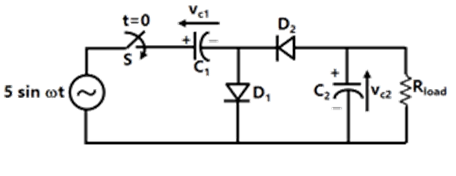


Sign in to see the solution
Log in to view the explanation, track your attempts, and keep your progress.
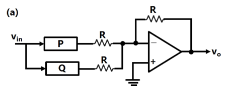
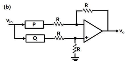
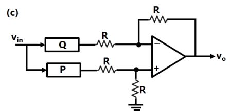
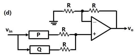
Sign in to UnlockThe block diagrams of two types of half wave rectifiers are shown in the figure. The transfer characteristics of the rectifiers are also shown within the block.
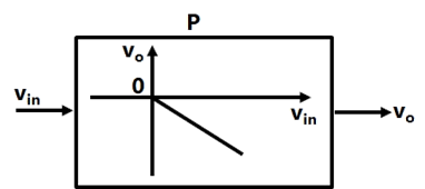
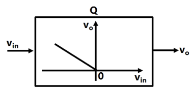
It is desired to make full wave rectifier using above two half-wave rectifiers. The resultant circuit will be
Sign in to see the solution
Log in to view the explanation, track your attempts, and keep your progress.
Sign in to UnlockWhat are the states of the three ideal diodes of the circuit shown in figure?
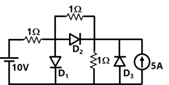
ON, OFF, OFF


OFF, ON, OFF
ON, OFF, ON
OFF, ON, ON
Sign in to see the solution
Log in to view the explanation, track your attempts, and keep your progress.
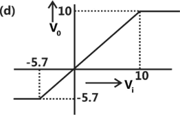
Sign in to UnlockAssuming the diodes and of the circuit shown in figure to be ideal ones, the transfer characteristics of the circuit will be
Sign in to see the solution
Log in to view the explanation, track your attempts, and keep your progress.
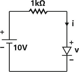
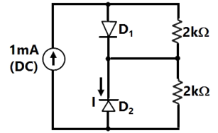
Sign in to UnlockAssume that and in Figure are ideal diodes. The value of current I is
Sign in to see the solution
Log in to view the explanation, track your attempts, and keep your progress.
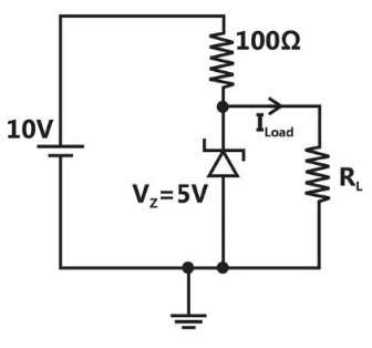
Sign in to UnlockThe current through the Zener diode in figure is

Sign in to see the solution
Log in to view the explanation, track your attempts, and keep your progress.
Sign in to UnlockThe circuit in figure shows a full-wave rectifier. The input voltage is 230V (RMS) single-phase ac. The peak reverse voltage across the diodes D1 and D2 is
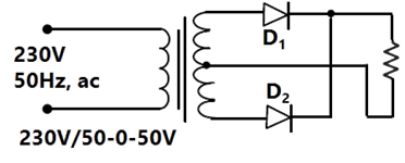

100 V
V

50 V
Sign in to see the solution
Log in to view the explanation, track your attempts, and keep your progress.
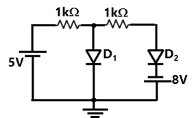
Sign in to UnlockAssuming that the diodes are ideal in figure, the current in is
Sign in to see the solution
Log in to view the explanation, track your attempts, and keep your progress.
Sign in to UnlockA voltage signal 10 sinωt is applied to the circuit with ideal diodes, as shown in Figure. The maximum and minimum values of the output waveform of the circuit are respectively 10kΩ

Sign in to see the solution
Log in to view the explanation, track your attempts, and keep your progress.
Sign in to UnlockThe forward resistance of the diode shown in Figure is 5Ω and the remaining parameters are same as those of an ideal diode. The dc component of the source current is


Sign in to see the solution
Log in to view the explanation, track your attempts, and keep your progress.
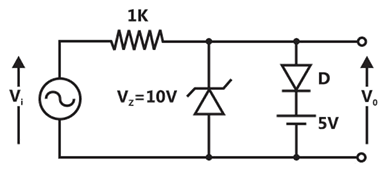
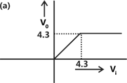
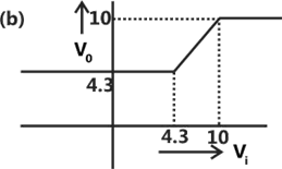
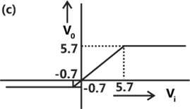
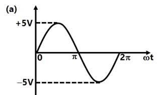
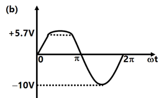
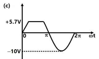
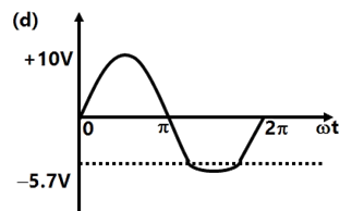
Sign in to UnlockThe cut-in voltage of both Zener diode and diode D shown in Figure is 0.7 V, while break down voltage of is 3.3 V and reverse breakdown voltage of D is 5V. The other parameters can be assumed to be the same as those of an ideal diode. The values of the peak output voltage are ........ ( Load Resistance = 1k Ohm )


Sign in to see the solution
Log in to view the explanation, track your attempts, and keep your progress.
Sign in to UnlockA diode whose terminal characteristics are related as , where is the reverse saturation current and is the thermal voltage , is biased at . Its dynamic resistance is:


Sign in to see the solution
Log in to view the explanation, track your attempts, and keep your progress.
Sign in to UnlockThe mobility of an electron in a conductor is expressed in terms of


Sign in to see the solution
Log in to view the explanation, track your attempts, and keep your progress.
Sign in to UnlockAs the temperature is increased, the voltage across a diode carrying a diode carrying a constant current
Sign in to see the solution
Log in to view the explanation, track your attempts, and keep your progress.
Sign in to UnlockThe depletion region or space charge region or transition in a semiconductor p-n junction diode has
Sign in to see the solution
Log in to view the explanation, track your attempts, and keep your progress.
Sign in to UnlockFigure shows an electric voltage regulator. The zener diode may be assumed to require a minimum current of 25 mA for satisfactory operations. The value of R required for satisfactory voltage regulation of the circuit is
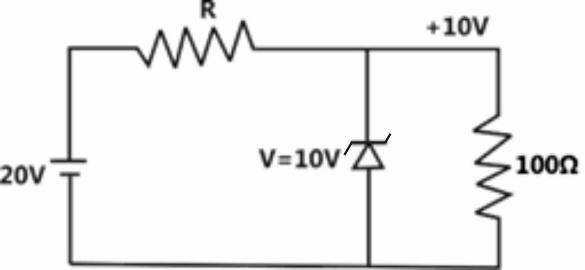
Sign in to see the solution
Log in to view the explanation, track your attempts, and keep your progress.
Sign in to Unlock