Analog Electronics
Diode and Its Applications
Rectifier Circuits
Questions mapped to Rectifier Circuits under Diode and Its Applications.
8
Total0
Attempted0
Correct0
IncorrectIn the circuit shown, the input is a sinusoidal AC voltage having an RMS value of 230V±20%. The worst-case peak-inverse voltage seen across any diode is _________ V. (Round off to 2 decimal places.)


Sign in to see the solution
Log in to view the explanation, track your attempts, and keep your progress.
Sign in to UnlockThe waveform shown in solid line is obtained by clipping a full-wave rectified sinusoid (shown dashed). The ratio of the RMS value of the full wave rectified waveform to the RMS value of the clipped waveform is _______.
(Round off to 2 decimal places.)

Sign in to see the solution
Log in to view the explanation, track your attempts, and keep your progress.
Sign in to UnlockFor the circuit shown in the figure below, assume that diodes are ideal.

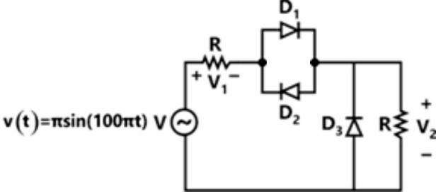
The DC components of voltages, respectively are

Sign in to see the solution
Log in to view the explanation, track your attempts, and keep your progress.
Sign in to UnlockIn the following circuit, the input voltage is 100. For , the average voltage across R (in volts) under steady – state is nearest to



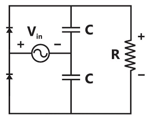
Sign in to see the solution
Log in to view the explanation, track your attempts, and keep your progress.
Sign in to UnlockIn the voltage doubler circuit shown in the figure, the switch 'S' is closed at t=0. Assuming diodes , and , to be ideal, load resistance to be infinite and initial capacitor voltages to be zero, the steady state voltage across capacitors , and , will be









Sign in to see the solution
Log in to view the explanation, track your attempts, and keep your progress.
Sign in to UnlockThe block diagrams of two types of half wave rectifiers are shown in the figure. The transfer characteristics of the rectifiers are also shown within the block.
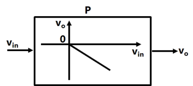
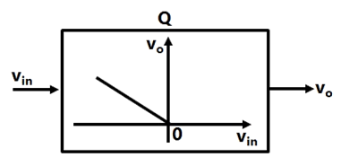
It is desired to make full wave rectifier using above two half-wave rectifiers. The resultant circuit will be
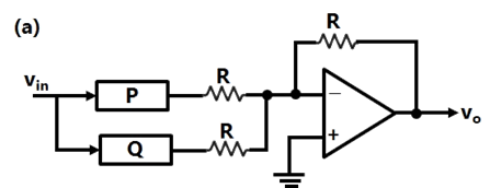
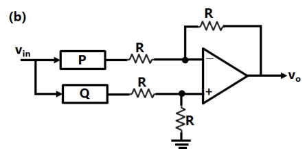
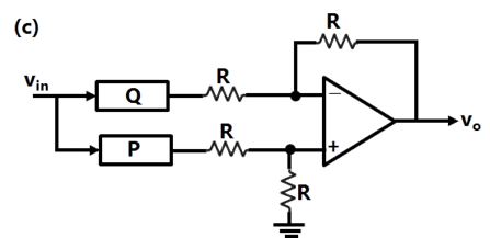
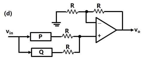
Sign in to see the solution
Log in to view the explanation, track your attempts, and keep your progress.
Sign in to UnlockThe circuit in figure shows a full-wave rectifier. The input voltage is 230V (RMS) single-phase ac. The peak reverse voltage across the diodes D1 and D2 is
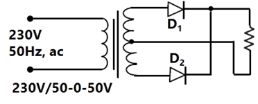

100 V
V

50 V
Sign in to see the solution
Log in to view the explanation, track your attempts, and keep your progress.
Sign in to UnlockThe forward resistance of the diode shown in Figure is 5Ω and the remaining parameters are same as those of an ideal diode. The dc component of the source current is





Sign in to see the solution
Log in to view the explanation, track your attempts, and keep your progress.
Sign in to Unlock