Analog Electronics
OP-AMP and its Applications
Negative feedback applications
Questions mapped to Negative feedback applications under OP-AMP and its Applications.
60
Total0
Attempted0
Correct0
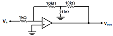
IncorrectIn the circuit shown, the open loop gain of the operational amplifier is .

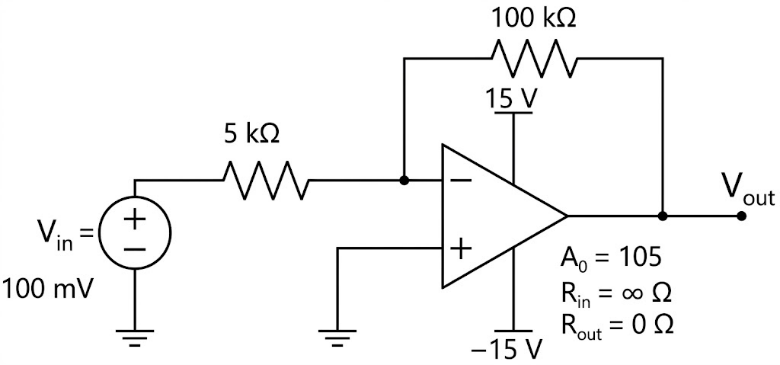
What is the voltage gain of the circuit? (Round off to two decimal places)
Sign in to see the solution
Log in to view the explanation, track your attempts, and keep your progress.
Sign in to UnlockThe op-amps in the following circuit are ideal. The voltage gain of the circuit is ________ (round off to the nearest integer).
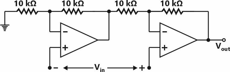
Sign in to see the solution
Log in to view the explanation, track your attempts, and keep your progress.
Sign in to UnlockA difference amplifier is shown in the figure. Assume the op-amp to be ideal. The CMRR (in ) of the difference amplifier is ________ (rounded off to 2 decimal places).

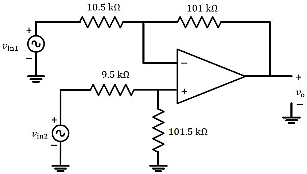
Sign in to see the solution
Log in to view the explanation, track your attempts, and keep your progress.
Sign in to UnlockThe steady State output of the circuit shown below, will

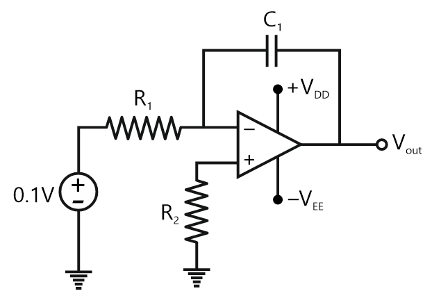
saturate to

saturate to

become equal to 0.1 V
become equal to -0.1 V
Sign in to see the solution
Log in to view the explanation, track your attempts, and keep your progress.
Sign in to UnlockThe current gain in the circuit with an ideal current amplifier given below is

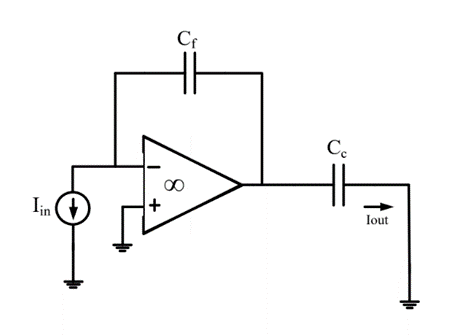




Sign in to see the solution
Log in to view the explanation, track your attempts, and keep your progress.
Sign in to UnlockIn the circuit below, the operational amplifier is ideal. If and , the output voltage () is



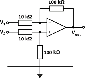
Sign in to see the solution
Log in to view the explanation, track your attempts, and keep your progress.
Sign in to UnlockThe op-amp shown in the figure is ideal. The input impedance is given by

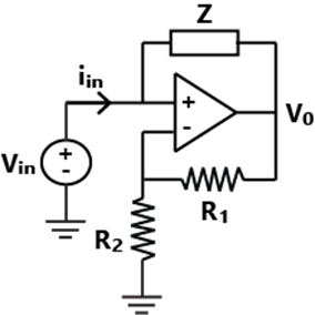


Z

Sign in to see the solution
Log in to view the explanation, track your attempts, and keep your progress.
Sign in to UnlockFor the circuit shown below, assume that the OPAMP is ideal
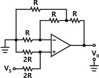




Sign in to see the solution
Log in to view the explanation, track your attempts, and keep your progress.
Sign in to UnlockThe circuit shown below is an example of a
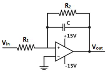
Sign in to see the solution
Log in to view the explanation, track your attempts, and keep your progress.
Sign in to UnlockFor the circuit shown below, taking the opamp as ideal, the output voltage in terms of the input voltages , and is



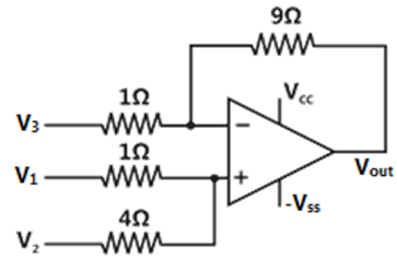




Sign in to see the solution
Log in to view the explanation, track your attempts, and keep your progress.
Sign in to UnlockOf the four characteristics given below, which are the major requirements for an instrumentation amplifier?
P. High common mode rejection ratio
Q. High input impedance.
R. High linearity.
S. High output impedance.
Sign in to see the solution
Log in to view the explanation, track your attempts, and keep your progress.
Sign in to UnlockConsider the circuit shown in the figure. In this circuit and . The input voltage is sinusoidal with a frequency of 50Hz, represented as a phasor with magnitude and phase angle 0 radian as shown in the figure. The output voltage is represented as a phasor with magnitude and phase angle radian. What is the value of the output phase angle (in radian) relative to the phase angle of the input voltage?





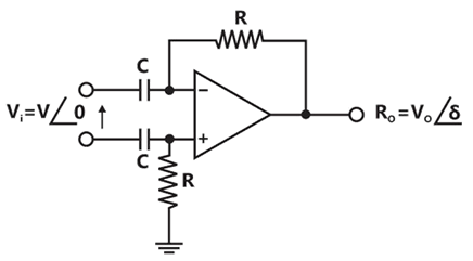
0



Sign in to see the solution
Log in to view the explanation, track your attempts, and keep your progress.
Sign in to UnlockThe op – amp shown in the figure has a finite gain A = 1000 and an infinite input resistance. A step voltage is applied at the input at time t=0 as shown. Assuming that the operational amplifier is not saturated, the time constant (in millisecond) of the output voltage is

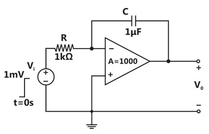
Sign in to see the solution
Log in to view the explanation, track your attempts, and keep your progress.
Sign in to UnlockThe operational amplifier shown in the figure is ideal. The input voltage (in Volt) is , The amplitude of the output voltage (in Volt) is____________.


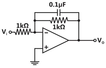
Sign in to see the solution
Log in to view the explanation, track your attempts, and keep your progress.
Sign in to UnlockGiven that the op – amps in the figure are ideal, the output voltage is
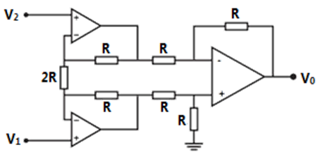




Sign in to see the solution
Log in to view the explanation, track your attempts, and keep your progress.
Sign in to UnlockAn operational-amplifier circuit is shown in the figure
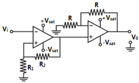
The output of the circuit for a given input is





Sign in to see the solution
Log in to view the explanation, track your attempts, and keep your progress.
Sign in to UnlockThe transfer characteristic of the op-amp circuit shown in figure is
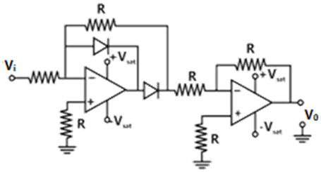
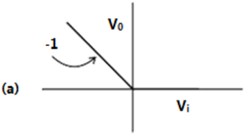
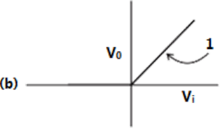
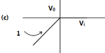
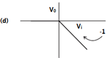
Sign in to see the solution
Log in to view the explanation, track your attempts, and keep your progress.
Sign in to UnlockIn the circuit shown below what is the output voltage in Volts if a silicon transistor Q and an ideal op-amp are used?

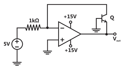
Sign in to see the solution
Log in to view the explanation, track your attempts, and keep your progress.
Sign in to UnlockIn the circuit shown below the op-amps are ideal. Then in Volts is
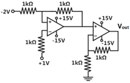
Sign in to see the solution
Log in to view the explanation, track your attempts, and keep your progress.
Sign in to UnlockThe circuit shown is a
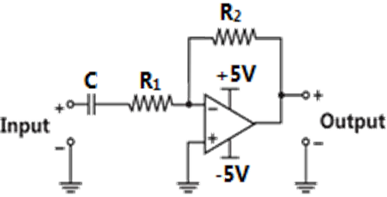
Low pass filter with

High pass filter with

Low pass filter with
High pass filter with
Sign in to see the solution
Log in to view the explanation, track your attempts, and keep your progress.
Sign in to UnlockA low-pass filter with a cut-off frequency of 30Hz is cascaded with a high-pass filter with a cut-off frequency of 20Hz. The resultant system of filters will function as
Sign in to see the solution
Log in to view the explanation, track your attempts, and keep your progress.
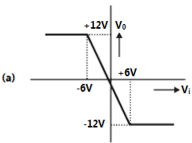
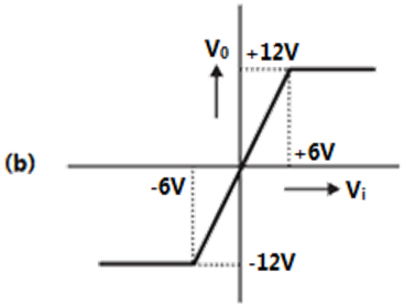
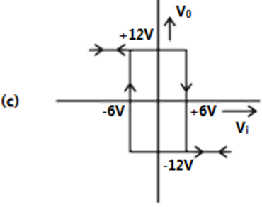
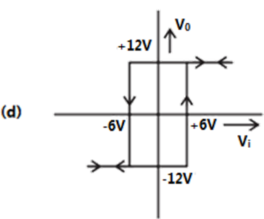
Sign in to UnlockFor the circuit shown below,
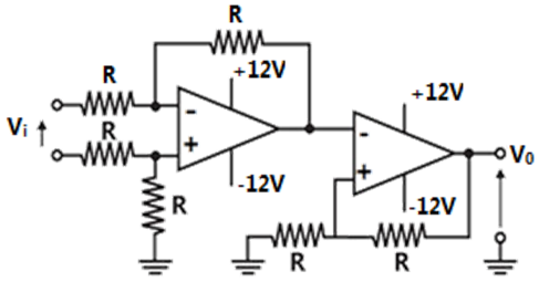
The correct transfer characteristics is
Sign in to see the solution
Log in to view the explanation, track your attempts, and keep your progress.
Sign in to UnlockGiven that the op-amp is ideal, the output voltage is

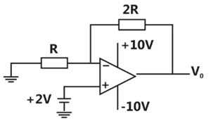
Sign in to see the solution
Log in to view the explanation, track your attempts, and keep your progress.
Sign in to UnlockThe following circuit has R = 10kΩ, C = 10µF. The input voltage is a sinusoid at 50Hz with an RMS value of 10V. Under ideal conditions, the current from the source is

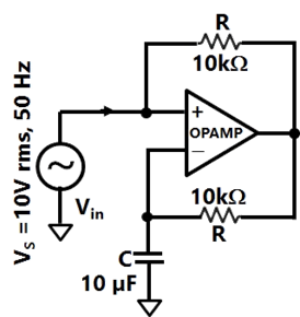
leading by 90°

leading by 90°

10mA leading by 90°
leading by 90°
Sign in to see the solution
Log in to view the explanation, track your attempts, and keep your progress.
Sign in to UnlockAn ideal op-amp circuit and its input waveform are shown in the figures. The output waveform of this circuit will be
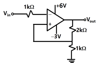
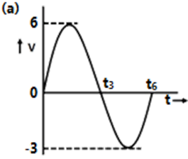
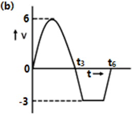
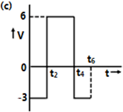
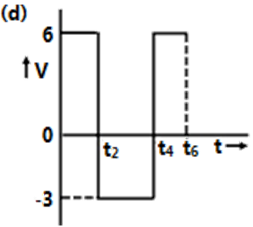
Sign in to see the solution
Log in to view the explanation, track your attempts, and keep your progress.
Sign in to UnlockA general filter circuit is shown in the figure:
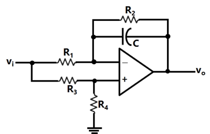
If and , the circuit acts as a


Sign in to see the solution
Log in to view the explanation, track your attempts, and keep your progress.
Sign in to UnlockA general filter circuit is shown in the figure:
The output of the filter is given to the circuit shown in figure:
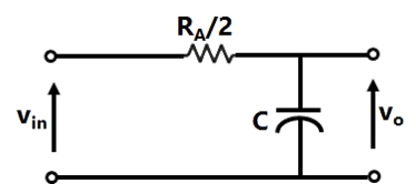
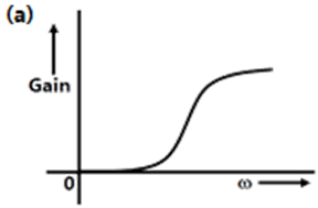
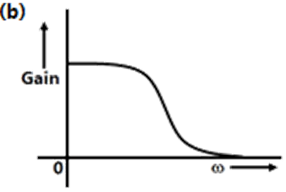
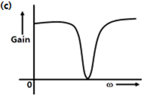
The gain vs frequency characteristic of the output will be

Sign in to see the solution
Log in to view the explanation, track your attempts, and keep your progress.
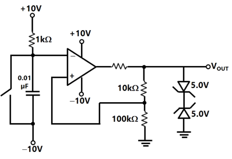
Sign in to UnlockThe switch S in the circuit of the figure is initially closed. It is opened at time t = 0. You may neglect the Zener diode forward voltage drops. What is the behavior of for t > 0?

Sign in to see the solution
Log in to view the explanation, track your attempts, and keep your progress.
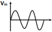
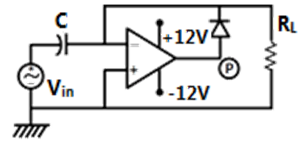
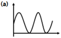
Sign in to UnlockFor a given sinusoidal input voltage, the voltage waveform at point P of the clamper circuit shown in figure will be
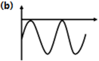
1
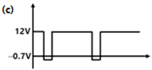
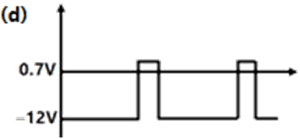
Sign in to see the solution
Log in to view the explanation, track your attempts, and keep your progress.
Sign in to UnlockThe parameters of the circuit shown in the figure are. If , then output voltage, input impedance and output impedance respectively are


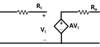




Sign in to see the solution
Log in to view the explanation, track your attempts, and keep your progress.
Sign in to UnlockConsider the inverting amplifier, using an ideal operational amplifier shown in Figure. The designer wishes to realize the input resistance seen by the small signal source to be as large as possible, while keeping the voltage gain between –10 and –25, the upper limit on is 1 MΩ. The value of should be


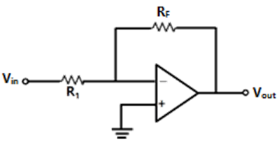
Infinity



Sign in to see the solution
Log in to view the explanation, track your attempts, and keep your progress.
Sign in to UnlockIn the active filter circuit shown in figure, if Q=1, a pair of poles will be realized with equal to

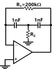
Sign in to see the solution
Log in to view the explanation, track your attempts, and keep your progress.
Sign in to UnlockThe input resistance of the circuit in figure is

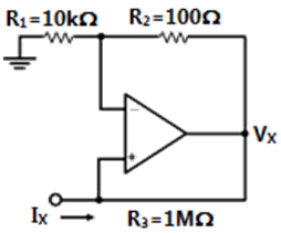




Sign in to see the solution
Log in to view the explanation, track your attempts, and keep your progress.
Sign in to UnlockFor the circuit of Figure with an ideal operational amplifier, the maximum phase shift of the output with reference to the input is

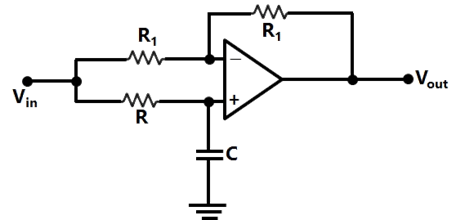
Sign in to see the solution
Log in to view the explanation, track your attempts, and keep your progress.
Sign in to UnlockAssuming the operational amplifier to be ideal, the gain for the circuit shown in Figure is

Sign in to see the solution
Log in to view the explanation, track your attempts, and keep your progress.
Sign in to UnlockA first order, low pass filter is given with and . What is the frequency at which the gain of the voltage transfer function of the filter is 0.25?


Sign in to see the solution
Log in to view the explanation, track your attempts, and keep your progress.
Sign in to UnlockAn op-amp has an open-loop gain of and an open-loop upper cutoff frequency of 10 Hz. If this op-amp is connected as an amplifier with a closed gain of 100, then the new upper cutoff frequency is

Sign in to see the solution
Log in to view the explanation, track your attempts, and keep your progress.
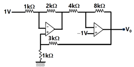
Sign in to UnlockFor the op-amp circuit shown in figure, determine the output voltage . Assume that the op-amps are ideal.
Sign in to see the solution
Log in to view the explanation, track your attempts, and keep your progress.
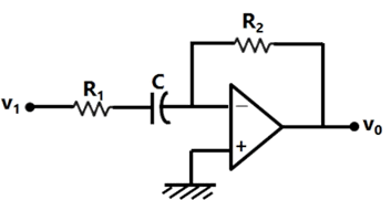
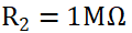
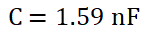
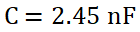
Sign in to UnlockA simple active filter is shown in Figure. Assume ideal op-amp. Derive the transfer function of the circuit, and state the type of the filter (i.e., high-pass, low-pass, band-pass, or band-reject). Determine the required values of , and C in order for the filter to have a 3-dB frequency of 1 kHz, a high frequency input resistance of 100 kΩ, and a high frequency gain magnitude of 10.



Sign in to see the solution
Log in to view the explanation, track your attempts, and keep your progress.
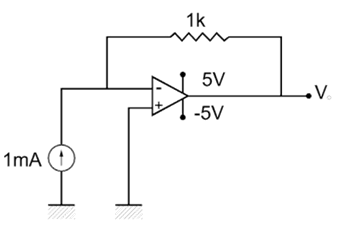
Sign in to UnlockThe circuit shown is fig. uses an ideal op-amp working +5V and -5V power supplies. The output voltage is equal to
Sign in to see the solution
Log in to view the explanation, track your attempts, and keep your progress.
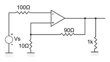
Sign in to UnlockThe feedback factor for the circuit shown in fig. is:




Sign in to see the solution
Log in to view the explanation, track your attempts, and keep your progress.
Sign in to UnlockAn active filter consisting of an op-amp, resistors and two capacitors of value C each, has a transfer function


Where

If and , determine the center frequency , gain and the Q of the filter.







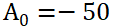
Sign in to see the solution
Log in to view the explanation, track your attempts, and keep your progress.
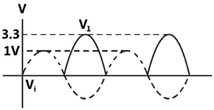
Sign in to UnlockThe input voltage in the circuit shown in fig is a 1 kHz sine wave of 1V amplitude. Assume ideal operational amplifiers with supply. Sketch on a single diagram the waveforms of the voltages and shown, indicating the peak value of and the average value

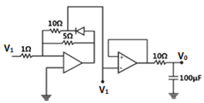
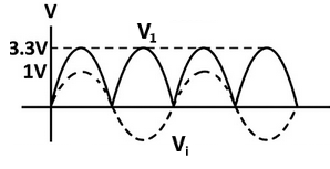
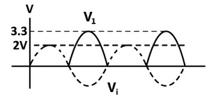
None
Sign in to see the solution
Log in to view the explanation, track your attempts, and keep your progress.
Sign in to UnlockMatch the column
Circuit
(a) (P) High-pass filter
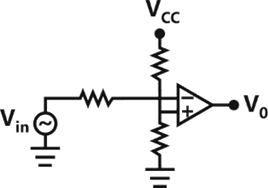
(b) (Q) Amplifier
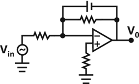
(c) (R) Comparator
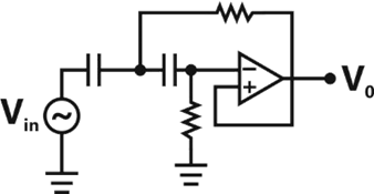
(S) Low-pass filter
Sign in to see the solution
Log in to view the explanation, track your attempts, and keep your progress.
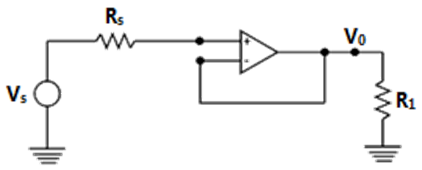
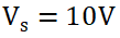
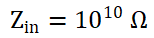
Sign in to UnlockIn the circuit shown in fig and, . For the op-amp, , R1 = 100 kΩ and R0 = 50Ω. For V0 = 10V, calculate and and estimate the input resistance of the circuit







Sign in to see the solution
Log in to view the explanation, track your attempts, and keep your progress.
Sign in to UnlockA major advantage of active filters is that they can be realized without using
Sign in to see the solution
Log in to view the explanation, track your attempts, and keep your progress.
Sign in to UnlockA differentiator has transfer function whose
Sign in to see the solution
Log in to view the explanation, track your attempts, and keep your progress.
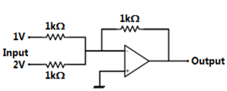
Sign in to UnlockThe circuit shown in figure, acts as a… and for the given inputs, its output voltage is… V
Sign in to see the solution
Log in to view the explanation, track your attempts, and keep your progress.
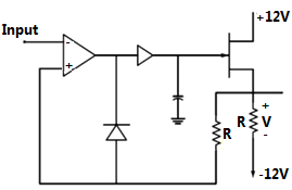
Sign in to UnlockFor an input signal 4sin10t, the voltage across the resistance R in the circuit shown in figure, is … V
Sign in to see the solution
Log in to view the explanation, track your attempts, and keep your progress.
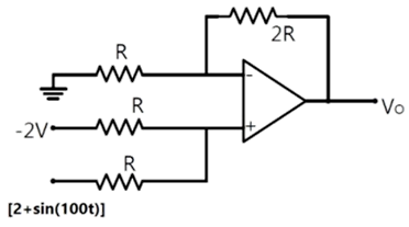
Sign in to UnlockA non-inverting Op-Amp amplifier is shown in figure. The output voltage is



None of these
Sign in to see the solution
Log in to view the explanation, track your attempts, and keep your progress.
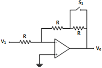
Sign in to UnlockLet the magnitude of the gain in the inverting OP-Amp amplifier circuit shown in be x with switch S1 open. When the switch S1 is closed the magnitude of gain becomes

–x
2x
-2x
Sign in to see the solution
Log in to view the explanation, track your attempts, and keep your progress.
Sign in to UnlockThe common mode voltage of a unity gain (voltage follower) op-amp buffer in terms of its output voltage is . ( True=1, False=0)

Sign in to see the solution
Log in to view the explanation, track your attempts, and keep your progress.
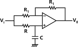
Sign in to UnlockFor the circuit shown in figure, determine and hence write the equations for the magnitude and phase response of . If the value of is 100k Ohm and of R is 10k Ohm, determine the value of C to obtain a phase shift to 270° between and for an input frequency of 1000rad/s.


Sign in to see the solution
Log in to view the explanation, track your attempts, and keep your progress.
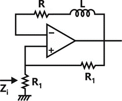
Sign in to UnlockFor the circuit shown in figure, determine the input impedance Z. assume the op-amp to be an ideal one.
R
2R

None
Sign in to see the solution
Log in to view the explanation, track your attempts, and keep your progress.
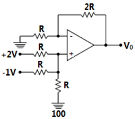
Sign in to UnlockGiven figure, shows a non-inverting op-amp summer with and . The output voltage __________________



Sign in to see the solution
Log in to view the explanation, track your attempts, and keep your progress.
Sign in to UnlockAn ideal OPAMP is used to make an inverting amplifier. The two input terminals of the OP-AMP are at the same potential because
Sign in to see the solution
Log in to view the explanation, track your attempts, and keep your progress.
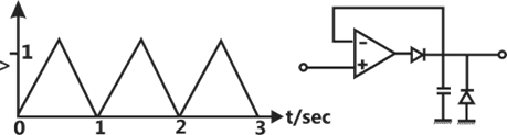
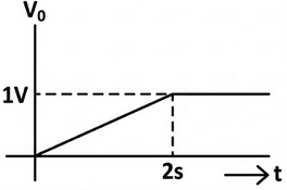
Sign in to UnlockThe circuit shown in figure is excited by the input shown in the figure. Sketch the waveform of the output also indicating the salient values. Assume all components to be ideal.
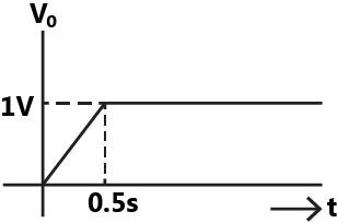
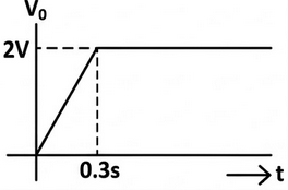
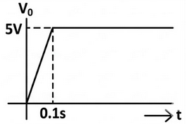
Sign in to see the solution
Log in to view the explanation, track your attempts, and keep your progress.
Sign in to UnlockIn the following circuit (figure.), the output V follows an equation of the form

Find a, b and f(t).
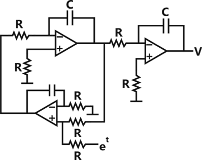


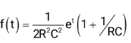
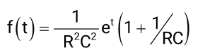
Sign in to see the solution
Log in to view the explanation, track your attempts, and keep your progress.
Sign in to UnlockWith ideal operational amplifiers, the circuit in figure simulates the output equation
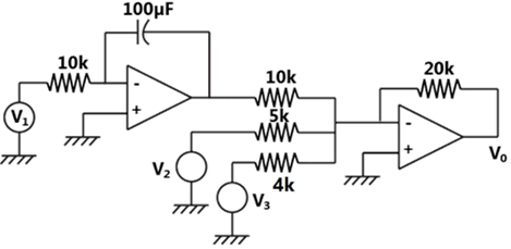




Sign in to see the solution
Log in to view the explanation, track your attempts, and keep your progress.
Sign in to UnlockIn figure shown, assume the Zener diode and the operational amplifier to be ideal.
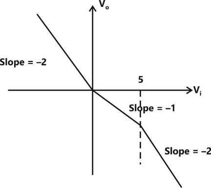
( gain )

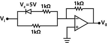
Gain characteristics

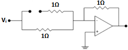
The equivalent circuit and the gain for
Gain = -2

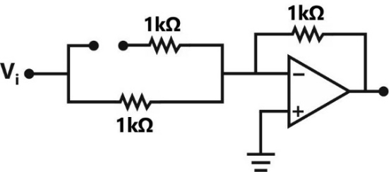
The equivalent circuit and the gain for
Gain = -1

The equivalent circuit for

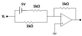
Sign in to see the solution
Log in to view the explanation, track your attempts, and keep your progress.
Sign in to Unlock