Analog Electronics
BJT
DC Analysis and Biasing Circuits of BJT
Questions mapped to DC Analysis and Biasing Circuits of BJT under BJT.
29
Total0
Attempted0
Correct0
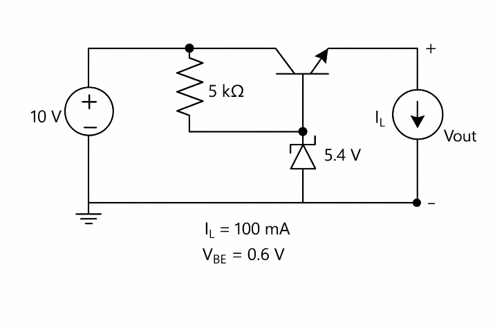
IncorrectIn the linear regulator circuit shown, the base to emitter voltage of the BJT is 0.6 V . The Zener diode clamps the base voltage to 5.4 V. Ignore the biasing current of the Zener diode and BJT.

The maximum possible efficiency of the regulator circuit is %

(Round off to one decimal place)
Sign in to see the solution
Log in to view the explanation, track your attempts, and keep your progress.
Sign in to UnlockA BJT biasing circuit is shown in the figure, where and . The Quiescent Point values of and are respectively




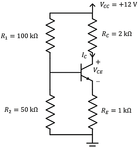
and


and

and


and
Sign in to see the solution
Log in to view the explanation, track your attempts, and keep your progress.
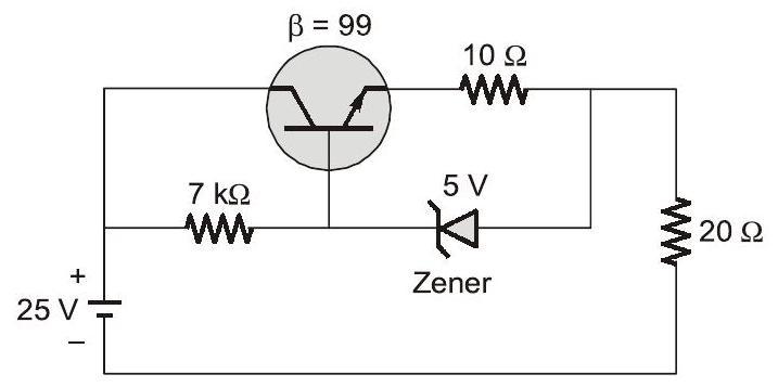
Sign in to UnlockThe Zener diode in circuit has a breakdown voltage of . The current gain of the transistor in the active region in 99. Ignore base-emitter voltage drop . The current through the 20Ω resistance in milliamperes is _________ (Round off to 2 decimal places).



Sign in to see the solution
Log in to view the explanation, track your attempts, and keep your progress.
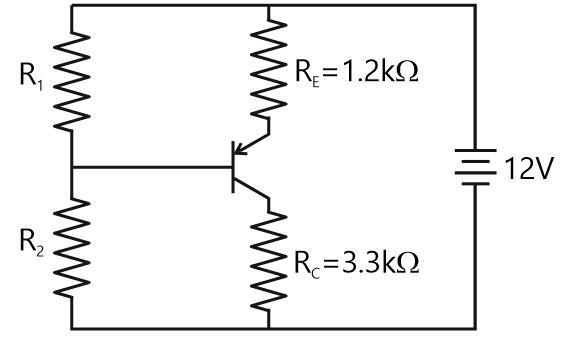
Sign in to UnlockIn the BJT circuit shown, beta of the PNP transistor is 100. Assume . .


The voltage across will be 5 V when is ……… kΩ. (Round off 2 decimal places)


Sign in to see the solution
Log in to view the explanation, track your attempts, and keep your progress.
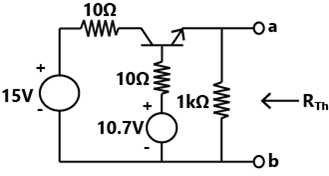
Sign in to UnlockIn the circuit shown in the figure, the bipolar junction transistor (BJT) has a current gain. The base-emitter voltage drop is a constant. The value of the Thevenin equivalent resistance (in ) as shown in the figure is ________(up to 2 decimal places).



Sign in to see the solution
Log in to view the explanation, track your attempts, and keep your progress.
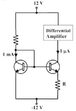
Sign in to UnlockThe circuit shown in the figure uses matched transistors with a thermal voltage . The base currents of the transistors are negligible. The value of the resistance R in that is required to provide 1 bias current for the differential amplifier block shown is __________ . (Give the answer up to one decimal place.)



Sign in to see the solution
Log in to view the explanation, track your attempts, and keep your progress.
Sign in to UnlockFor the circuit shown in the figure below, it is given that . The transistor has and when the B-E junction is forward biased.



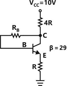
For this circuit, the value of is

Sign in to see the solution
Log in to view the explanation, track your attempts, and keep your progress.
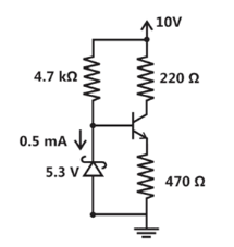
Sign in to UnlockA transistor circuit is given below. The Zener diode breakdown voltage is 5.3V as shown. Take base to emitter voltage drop to be 0.6V. The value of the current gain is __________.

Sign in to see the solution
Log in to view the explanation, track your attempts, and keep your progress.
Sign in to UnlockIn the given circuit, the silicon transistor has and a collector voltage . Then the ratio of and is ____________.



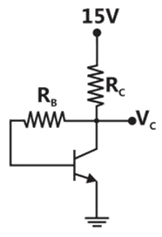
Sign in to see the solution
Log in to view the explanation, track your attempts, and keep your progress.
Sign in to UnlockWhen a bipolar junction transistor is operating in the saturation mode, which one of the following statements is TRUE about the state of its collector – base (CB) and the base – emitter (BE) junctions?
Sign in to see the solution
Log in to view the explanation, track your attempts, and keep your progress.
Sign in to UnlockThe transistor in the given circuit should always be in active region. Take , . The maximum value of RC in which can be used, is __________.



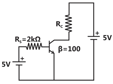
Sign in to see the solution
Log in to view the explanation, track your attempts, and keep your progress.
Sign in to UnlockThe transistor used in the circuit shown below has a of 30 and is negligible.

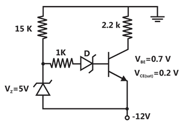
If the forward voltage drop of diode is 0.7V, then the current through collector will be
Sign in to see the solution
Log in to view the explanation, track your attempts, and keep your progress.
Sign in to UnlockThe transistor circuit shown uses a silicon transistor with and a dc current gain of 100. The value of is


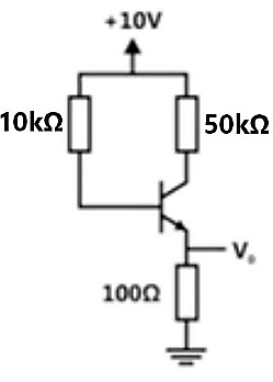
Sign in to see the solution
Log in to view the explanation, track your attempts, and keep your progress.
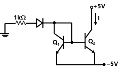
Sign in to UnlockTwo perfectly matched silicon transistors are connected as shown in the figure. Assuming the β of the transistors to be very high and the forward voltage drop in diodes to be 0.7V, the value of current I is
Sign in to see the solution
Log in to view the explanation, track your attempts, and keep your progress.
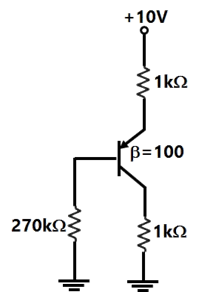
Sign in to UnlockThe common emitter forward current gain of the transistor shown is .

The transistor is operating in
Sign in to see the solution
Log in to view the explanation, track your attempts, and keep your progress.
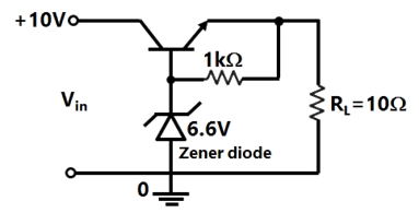
Sign in to UnlockThe three-terminal linear voltage regulator is connected to a load resistor as shown in the figure. If is 10 V, what is the power dissipated in the transistor?


Sign in to see the solution
Log in to view the explanation, track your attempts, and keep your progress.
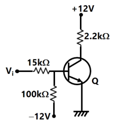
Sign in to UnlockConsider the circuit shown in figure. If the β of the transistor is 39 and is 20nA and the input voltage is +5V, then transistor would be operating in
Sign in to see the solution
Log in to view the explanation, track your attempts, and keep your progress.
Sign in to UnlockThe common emitter amplifier shown in Figure is biased using a 1mA ideal current source. The approximate base current value is:
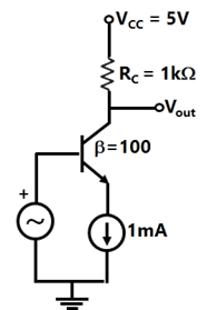
Sign in to see the solution
Log in to view the explanation, track your attempts, and keep your progress.
Sign in to UnlockTwo perfectly matched silicon transistors are connected as shown in figure. The value of the current I is
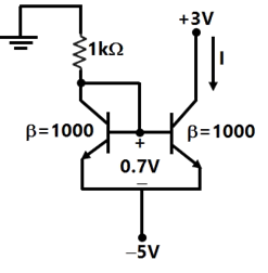
Sign in to see the solution
Log in to view the explanation, track your attempts, and keep your progress.
Sign in to UnlockA bipolar junction transistor (BJT) is used as a power control switch by biasing it in the cut-off region (OFF state) or in the saturation region (ON state). In the ON state, for the BJT
Sign in to see the solution
Log in to view the explanation, track your attempts, and keep your progress.
Sign in to UnlockIn the Schmitt trigger circuit shown in figure, if , the output logic low level is


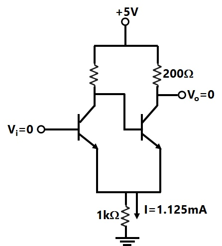
Sign in to see the solution
Log in to view the explanation, track your attempts, and keep your progress.
Sign in to UnlockIn the circuit of Figure, assume that the transistor has . The value of collector current of the transistor is approximately


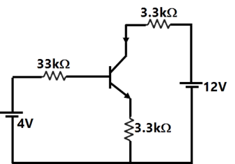
Sign in to see the solution
Log in to view the explanation, track your attempts, and keep your progress.
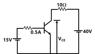
Sign in to UnlockIn the circuit shown in Figure, the current gain (β) of the ideal transistor is 10. The operating point of the transistor is

Sign in to see the solution
Log in to view the explanation, track your attempts, and keep your progress.
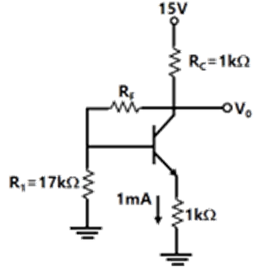
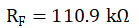
Sign in to UnlockFor the circuit shown in Figure, and . Determine






Sign in to see the solution
Log in to view the explanation, track your attempts, and keep your progress.
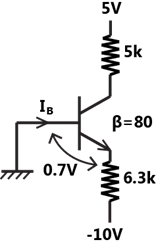
Sign in to UnlockIn the circuit of fig, the value of the base current will be

Sign in to see the solution
Log in to view the explanation, track your attempts, and keep your progress.
Sign in to UnlockOne of the applications of current mirror is:
Sign in to see the solution
Log in to view the explanation, track your attempts, and keep your progress.
Sign in to UnlockA NPN, silicon transistor is meant for low-current audio amplification. Match its following characteristics against their values:
Characteristics Values
(a) (P) 0.7V

(b) (Q) 0.2V

(c) (R) 6V

(S) 50V
Sign in to see the solution
Log in to view the explanation, track your attempts, and keep your progress.
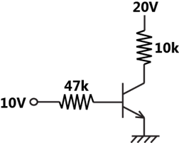
Sign in to UnlockIn the transistor circuit shown in figure, collector-to-ground voltage is +20V. Which of the following is the probable cause of error?
Sign in to see the solution
Log in to view the explanation, track your attempts, and keep your progress.
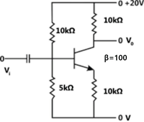
Sign in to UnlockFigure below shows a common emitter amplifier. The quiescent collector voltage of the circuit is approximately

10 V
14 V
20 V
Sign in to see the solution
Log in to view the explanation, track your attempts, and keep your progress.
Sign in to Unlock