Digital Electronics
Combinational Circuits
Other Circuits
Questions mapped to Other Circuits under Combinational Circuits.
17
Total0
Attempted0
Correct0
IncorrectThe output expression for the Karnaugh map shown below is





Sign in to see the solution
Log in to view the explanation, track your attempts, and keep your progress.
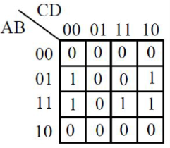
Sign in to UnlockThe output expression for the Karnaugh map shown below is




Sign in to see the solution
Log in to view the explanation, track your attempts, and keep your progress.
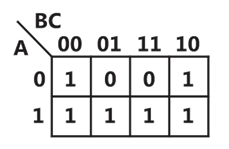
Sign in to UnlockThe output expression for the Karnaugh map shown below is




Sign in to see the solution
Log in to view the explanation, track your attempts, and keep your progress.
Sign in to Unlock(0,1,3,4,5,7,9,11,12,13,14,15) is a maxterm representation of a Boolean function f(A,B,C,D) where A is the MSB and D is the LSB. The equivalent minimized representation of this function is





Sign in to see the solution
Log in to view the explanation, track your attempts, and keep your progress.
Sign in to UnlockConsider the following sum of products expression, F.

The equivalent product of sums expressions is




Sign in to see the solution
Log in to view the explanation, track your attempts, and keep your progress.
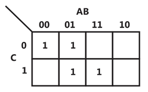
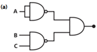
Sign in to UnlockWhich of the following logic circuits is a realization of the function F whose Karnaugh map is shown in figure
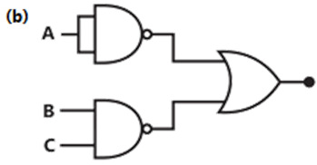
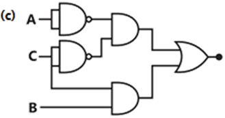
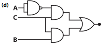
Sign in to see the solution
Log in to view the explanation, track your attempts, and keep your progress.
Sign in to UnlockThe SOP (sum off products) form of a Boolean function is , where inputs are A, B, C, D (A is MSB, and D is LSB). The equivalent minimized expression of the function is





Sign in to see the solution
Log in to view the explanation, track your attempts, and keep your progress.
Sign in to UnlockA state diagram of a logic gate which exhibits a delay in the output is shown in the figure, where X is the don’t care condition, and Q is the output representing the state.
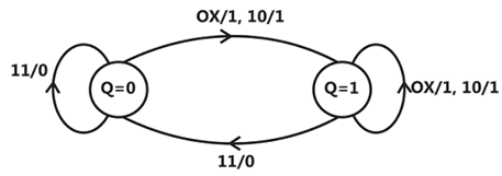
The logic gate represented by the gate diagram is
Sign in to see the solution
Log in to view the explanation, track your attempts, and keep your progress.
Sign in to UnlockIn the sum of products function, the prime implicant’s are





Sign in to see the solution
Log in to view the explanation, track your attempts, and keep your progress.
Sign in to UnlockThe output Y of a 2-bit comparator is logic 1 whenever the 2-bit input A is greater than the 2-bit input B. The number of combinations for which the output is logic 1, is
Sign in to see the solution
Log in to view the explanation, track your attempts, and keep your progress.
Sign in to UnlockThe following Karnaugh map represents a function F.
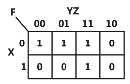
A minimized form of the function F is




Sign in to see the solution
Log in to view the explanation, track your attempts, and keep your progress.
Sign in to UnlockThe following Karnaugh map represents a function F.
Which of the following circuits is a realization of the above function F?
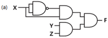
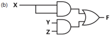

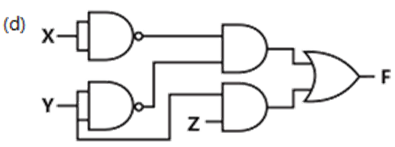
Sign in to see the solution
Log in to view the explanation, track your attempts, and keep your progress.
Sign in to UnlockA, B, C and D are input bits, and Y is the output bit in the XOR gate circuit of the figure below. Which of the following statements about the sum S of A. B, C, D and Y is correct?
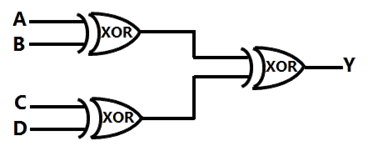
Sign in to see the solution
Log in to view the explanation, track your attempts, and keep your progress.
Sign in to UnlockA digital circuit, which compares two numbers, is shown in figure. To get output Y = 0, choose one pair of correct input numbers.

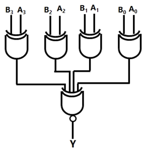
Sign in to see the solution
Log in to view the explanation, track your attempts, and keep your progress.
Sign in to UnlockThe minimal product of sums function described by the K-map
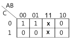
Sign in to see the solution
Log in to view the explanation, track your attempts, and keep your progress.
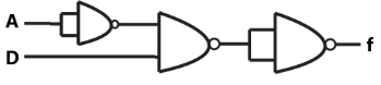
Sign in to UnlockIn a digital combinational circuit with 4 inputs (A, B, C, D), it is required to obtain an output of logical 1 only for the input combination (A=1; B=C=D=0). It is known that the following combinations of input are forbidden:
ABCD= 1010, 1011, 1100, 1101, 1110, 1111
Evaluate the logical expression for the output and realize the same with two input NAND gates. Assume that complements of inputs are not available.
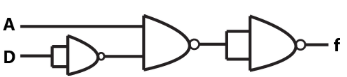

None
Sign in to see the solution
Log in to view the explanation, track your attempts, and keep your progress.
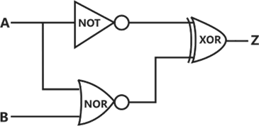
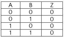
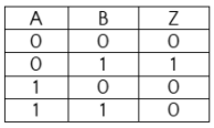
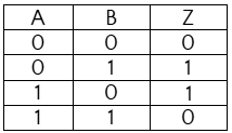
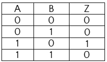
Sign in to UnlockComplete the truth table for the combinational circuit shown in figure.

Sign in to see the solution
Log in to view the explanation, track your attempts, and keep your progress.
Sign in to Unlock