Analog Electronics
MOSFET
DC Analysis and Biasing Circuits of MOSFET
Questions mapped to DC Analysis and Biasing Circuits of MOSFET under MOSFET.
10
Total0
Attempted0
Correct0
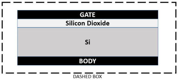
IncorrectThe cross-section of a metal-oxide-semiconductor structure is shown schematically. Starting from an uncharged condition, a bias of +3 V is applied to the gate contact with respect to the body contact. The charge inside the silicon dioxide layer is then measured to be +Q. The total charge contained within the dashed box shown, upon
application of bias, expressed as a multiple of Q (absolute value in Coulombs, rounded off to the nearest integer) is ___________.
Sign in to see the solution
Log in to view the explanation, track your attempts, and keep your progress.
Sign in to UnlockGiven is the gate-source voltage, is the drain source voltage, and is the threshold voltage of an enhancement type NMOS transistor, the conditions for transistor to be biased in saturation are







Sign in to see the solution
Log in to view the explanation, track your attempts, and keep your progress.
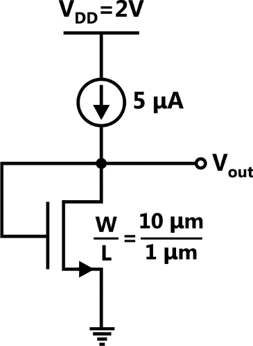
Sign in to UnlockThe enhancement type MOSFET in the circuit below operates according to the square law. , the threshold voltage is 500 mV. Ignore channel length modulation. The output voltage is



Sign in to see the solution
Log in to view the explanation, track your attempts, and keep your progress.
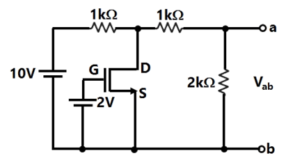
Sign in to UnlockAssume that the N-channel MOSFET shown in Figure is ideal, and that its threshold voltage is +1.0V. The voltage between nodes a and b is:

Sign in to see the solution
Log in to view the explanation, track your attempts, and keep your progress.
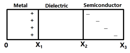
Sign in to UnlockThe charge distribution in a metal-dielectric-semiconductor specimen is shown in Figure. The negative charge density decreases linearly in the semiconductor as shown. The electric field distribution is as shown in
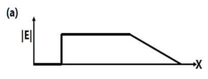
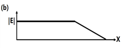
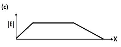
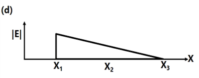
Sign in to see the solution
Log in to view the explanation, track your attempts, and keep your progress.
Sign in to UnlockThe value of R for which the PMOS transistor in figure will be biased in linear region is
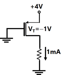




Sign in to see the solution
Log in to view the explanation, track your attempts, and keep your progress.
Sign in to UnlockThe variation of drain current with gate-to-source voltage ( characteristic) of a MOSFET is shown in Figure. The MOSFET is

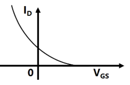
Sign in to see the solution
Log in to view the explanation, track your attempts, and keep your progress.
Sign in to UnlockFor the n-channel enhancement MOSFET shown in Figure, the threshold voltage . The drain current of the MOSFET is 4 mA when the drain resistance is . If the value of is increased to , drain current will become





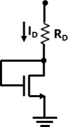
Sign in to see the solution
Log in to view the explanation, track your attempts, and keep your progress.
Sign in to UnlockAn n-channel JFET, having a pinch off voltage of −5V, shows a trans-conductance of 1mA/V when the applied gate-to-source voltage is -3V. Its maximum trans-conductance (in mA/V) is



Sign in to see the solution
Log in to view the explanation, track your attempts, and keep your progress.
Sign in to UnlockAn enhancement type n-channel MOSFET is represented by the symbol
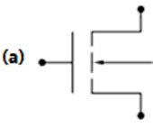
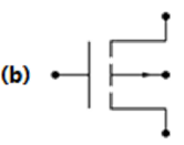
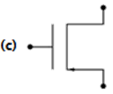
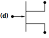
Sign in to see the solution
Log in to view the explanation, track your attempts, and keep your progress.
Sign in to Unlock