Power Electronics
Power Semiconductor Devices
Switch Characteristics
Questions mapped to Switch Characteristics under Power Semiconductor Devices.
21
Total0
Attempted0
Correct0
IncorrectThe figure shows a straight-line approximation for the forward characteristics of a power diode. A continuous on-state current of 15 A is flowing through the diode.
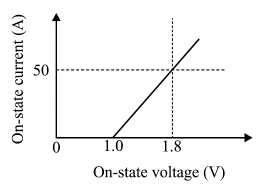
What is the power loss in the diode?
Sign in to see the solution
Log in to view the explanation, track your attempts, and keep your progress.
Sign in to UnlockIf the following switching devices have similar power ratings, which one of them is the fastest?
Sign in to see the solution
Log in to view the explanation, track your attempts, and keep your progress.
Sign in to UnlockA semiconductor switch needs to block voltage of only one polarity during OFF state as shown in figure (i) and carry current in both directions during ON state as shown in figure (ii). Which of the following switch combination(s) will realize the same?


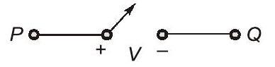
Fig. (i)
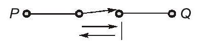
Fig. (ii)
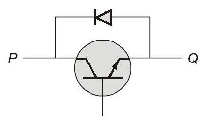
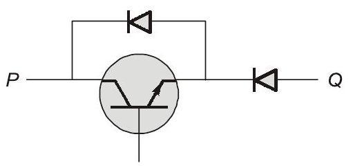
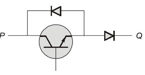
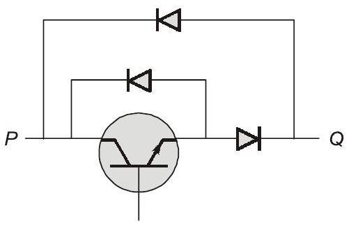
Sign in to see the solution
Log in to view the explanation, track your attempts, and keep your progress.
Sign in to UnlockA charger supplies 100 W at 20 V for charging the battery of a laptop. The power devices, used in the converter inside the charger, operate at a switching frequency of 200 kHz. Which power device is best suited for this purpose?
Sign in to see the solution
Log in to view the explanation, track your attempts, and keep your progress.
Sign in to UnlockA double pulse measurement for an inductively loaded circuit controlled by the IGBT switch is carried out to evaluate the reverse recovery characteristics of the diode. D, represented approximately as a piecewise linear plot of current vs time at diode turn-off. is a parasitic inductance due to the wiring of the circuit, and is in series with the diode. The point on the plot (indicate your choice by entering 1, 2, 3 or 4) at which the IGBT experiences the highest current stress is

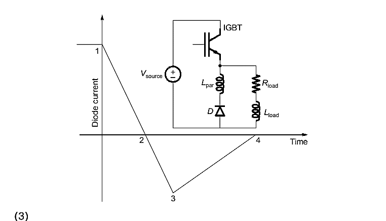
Sign in to see the solution
Log in to view the explanation, track your attempts, and keep your progress.
Sign in to UnlockFour power semiconductor devices are shown in the figure along with their relevant terminals. The device(s) that can carry dc current continuously in the direction shown when gated appropriately is (are)

Sign in to see the solution
Log in to view the explanation, track your attempts, and keep your progress.
Sign in to UnlockFor the power semiconductor devices IGBT, MOSFET, Diode and Thyristor, which one of the following statements is TRUE?
Sign in to see the solution
Log in to view the explanation, track your attempts, and keep your progress.
Sign in to UnlockA steady dc current of 100A is flowing through a power module (S, D) as shown in Figure (a). The V-I characteristics of the IGBT (S) and the diode (D) are shown in the Figure (b) and (c), respectively. The conduction power loss in the power module (S, D), in watts, is ________________.

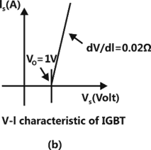
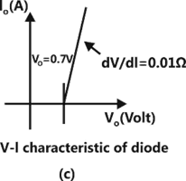
Sign in to see the solution
Log in to view the explanation, track your attempts, and keep your progress.
Sign in to UnlockThe voltage across and the current through a semiconductor switch during a turn-ON transition are shown in figure. The energy dissipated during the turn-ON transition, in mJ, is ____________.


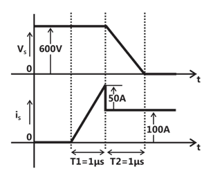
Sign in to see the solution
Log in to view the explanation, track your attempts, and keep your progress.
Sign in to UnlockFigure shows four electronic switches (i), (ii), (iii) and (iv). Which of the switches can block voltages of either polarity (applied between terminals ‘a’ and ‘b’) when the active device is in the OFF state?
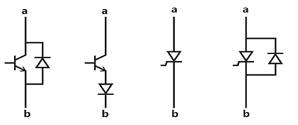
(i) (ii) (iii) (iv)
Sign in to see the solution
Log in to view the explanation, track your attempts, and keep your progress.
Sign in to UnlockFigure shows a composite switch consisting of a power transistor (BJT) in series with a diode. Assuming that the transistor switch and the diode are ideal, the I-V characteristics of the composite switch is
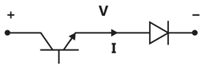
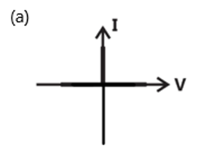
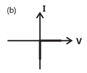
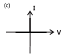
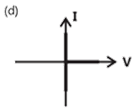
Sign in to see the solution
Log in to view the explanation, track your attempts, and keep your progress.
Sign in to UnlockThe L-C circuit shown in the figure has an impedance L = I mH and a capacitance C = 10uF.
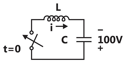
The initial current through the inductor is zero, while the initial capacitor voltage is 100V. The switch is closed at t = 0. The current i through the circuit is:




Sign in to see the solution
Log in to view the explanation, track your attempts, and keep your progress.
Sign in to UnlockMatch the switch arrangements on the top row to the steady-state V-I characteristics on the lower row. The steady state operating points are shown by large black dots.




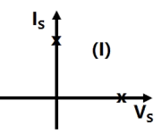
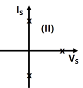
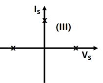
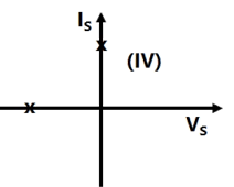
Sign in to see the solution
Log in to view the explanation, track your attempts, and keep your progress.
Sign in to UnlockThe conduction loss versus device current characteristic of a power MOSFET is best approximated by
Sign in to see the solution
Log in to view the explanation, track your attempts, and keep your progress.
Sign in to UnlockFigure shows the voltage across a power semiconductor device and the current through the device during a switching transition. Is the transition a turn ON transition or a turn OFF transition? What is the energy lost during the transition?
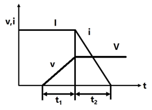
Turn ON,

Turn OFF,

Turn ON,
Turn OFF,
Sign in to see the solution
Log in to view the explanation, track your attempts, and keep your progress.
Sign in to UnlockA MOSFET rated for 15 A, carries a periodic current as shown in figure. The ON state resistance of the MOSFET is 0.15Ω. The average ON state loss in the MOSFET is
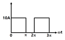
Sign in to see the solution
Log in to view the explanation, track your attempts, and keep your progress.
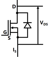
Sign in to UnlockFigure shown a MOSFET with an integral body diode. It is employed as a power switching device in the ON and OFF states through appropriate control. The ON and OFF states of the switch are given on the plane by

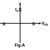
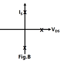

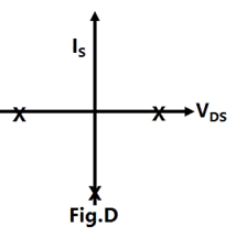
Sign in to see the solution
Log in to view the explanation, track your attempts, and keep your progress.
Sign in to UnlockThe MOSFET switch in its on-state may be considered equivalent to:
Sign in to see the solution
Log in to view the explanation, track your attempts, and keep your progress.
Sign in to UnlockWhich semiconductor power device out of the following is not a current triggered device?
Sign in to see the solution
Log in to view the explanation, track your attempts, and keep your progress.
Sign in to UnlockThe thermal resistance between the body of a power semiconductor device and the ambient is expressed as
Sign in to see the solution
Log in to view the explanation, track your attempts, and keep your progress.
Sign in to UnlockIn the circuit of figure, the switch ‘S’ is closed at t=0 with . In the steady state equals


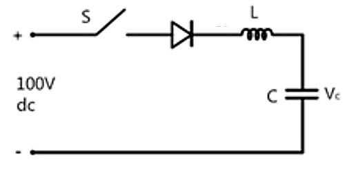
Sign in to see the solution
Log in to view the explanation, track your attempts, and keep your progress.
Sign in to Unlock