Analog Electronics
Amplifiers
Practice questions from Amplifiers.
54
Total0
Attempted0
Correct0
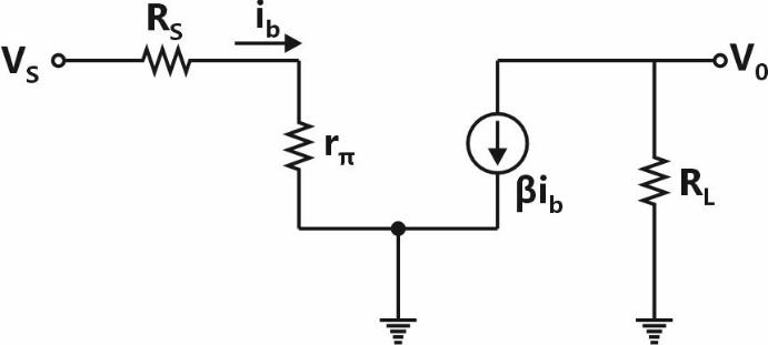
IncorrectA simplified small-signal equivalent circuit of a BJT-based amplifier is given below.
The small-signal voltage gain in is _________.


Sign in to see the solution
Log in to view the explanation, track your attempts, and keep your progress.
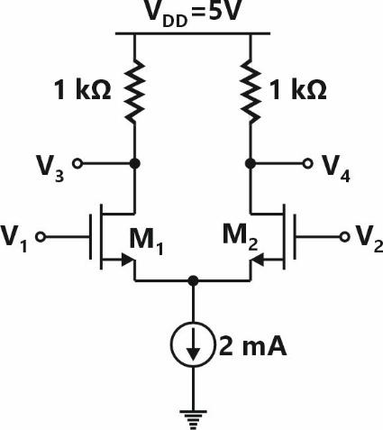
Sign in to UnlockThe identical MOSFETs and in the circuit given below are ideal and biased in the saturation region. and have a transconductance of 5 mS .


The input signals (in Volts) are:


The output signal (in Volts) is __________.


Sign in to see the solution
Log in to view the explanation, track your attempts, and keep your progress.
Sign in to UnlockA good transimpedance amplifier has
Sign in to see the solution
Log in to view the explanation, track your attempts, and keep your progress.
Sign in to UnlockNegative feedback in a closed-loop control system DOES NOT
Sign in to see the solution
Log in to view the explanation, track your attempts, and keep your progress.
Sign in to UnlockIn the circuit shown, . Transistors and are identical. Assume that the thermal voltage is 26 mV at. At the value of the voltage (in mV) is _______.


Sign in to see the solution
Log in to view the explanation, track your attempts, and keep your progress.
Sign in to UnlockA good current buffer has
Sign in to see the solution
Log in to view the explanation, track your attempts, and keep your progress.
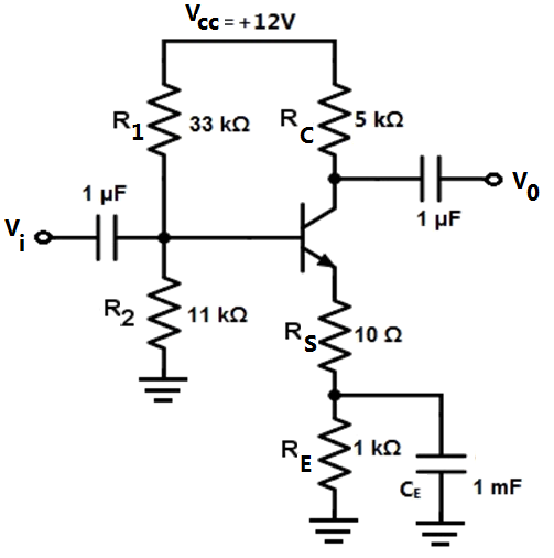
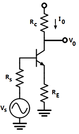
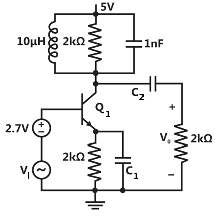
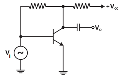
Sign in to UnlockFor the amplifier shown in the figure, the BJT parameters are, β = 200, and thermal voltage. The voltage gain () of the amplifier is _______.


Sign in to see the solution
Log in to view the explanation, track your attempts, and keep your progress.
Sign in to UnlockThe feedback topology in the amplifier circuit (the base bias circuit is not shown for simplicity) in the figure is
Sign in to see the solution
Log in to view the explanation, track your attempts, and keep your progress.
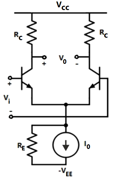
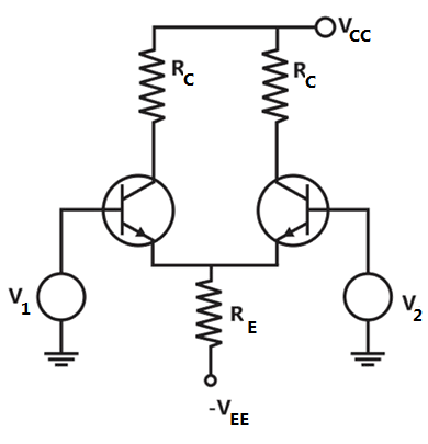
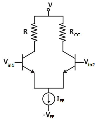
Sign in to UnlockIn the differential amplifier shown in the figure, the magnitudes of the common-mode and differential-mode gains are and, respectively. If the resistance is increased, then


Increases

common-mode rejection ratio increases
Increases

common-mode rejection ratio decrease
Sign in to see the solution
Log in to view the explanation, track your attempts, and keep your progress.
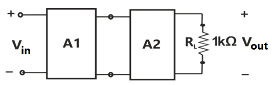
Sign in to UnlockA cascade connection of two voltage amplifiers A1 and A2 is shown in the figure. The open-loop gain, input resistance, and output resistance for A1 and A2 are as follows:


A1: = 10, = 10 kΩ, = 1 kΩ.
A2: = 5, = 5 kΩ, = 200 Ω.
The approximate overall voltage gain is _________.

Sign in to see the solution
Log in to view the explanation, track your attempts, and keep your progress.
Sign in to UnlockThe desirable characteristics of a trans-conductance amplifier are
Sign in to see the solution
Log in to view the explanation, track your attempts, and keep your progress.
Sign in to UnlockIf the emitter resistance in a common-emitter voltage amplifier is not bypassed, it will
Sign in to see the solution
Log in to view the explanation, track your attempts, and keep your progress.
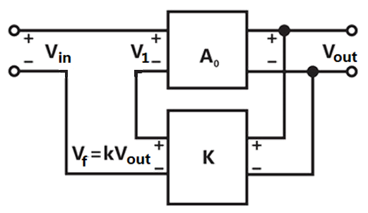
Sign in to UnlockIn a voltage-voltage feedback as shown below, which one of the following statements is TRUE if the gain k is increased?
Sign in to see the solution
Log in to view the explanation, track your attempts, and keep your progress.
Sign in to UnlockIn the circuit shown below, capacitors and are very large and are shorts at the input frequency. is a small signal input. The gain magnitude at 10 Mrad/s is


Sign in to see the solution
Log in to view the explanation, track your attempts, and keep your progress.
Sign in to UnlockIn a transconductance amplifier, it is desirable to have
Sign in to see the solution
Log in to view the explanation, track your attempts, and keep your progress.
Sign in to UnlockThe input impedance and the output impedance of an ideal trans-conductance (voltage controlled current source) amplifier are


,


,

,

,
Sign in to see the solution
Log in to view the explanation, track your attempts, and keep your progress.
Sign in to UnlockThe effect of current shunt feedback in an amplifier is to
Sign in to see the solution
Log in to view the explanation, track your attempts, and keep your progress.
Sign in to UnlockIn an ideal differential amplifier shown in figure, a large value of

Sign in to see the solution
Log in to view the explanation, track your attempts, and keep your progress.
Sign in to UnlockVoltage series feedback (also called series shunt feedback) results in
Sign in to see the solution
Log in to view the explanation, track your attempts, and keep your progress.
Sign in to UnlockIf the differential voltage gain and the common mode voltage gain of a differential amplifier are 48 dB and 2 dB respectively, then its common mode rejection ratio is
Sign in to see the solution
Log in to view the explanation, track your attempts, and keep your progress.
Sign in to UnlockAn amplifier without feedback has a voltage gain of 50, input resistance of 1 KΩ and output resistance of 2.5 KΩ. The input resistance of the current-shunt negative feedback amplifier using the above amplifier with a feedback factor of 0.2, is


Sign in to see the solution
Log in to view the explanation, track your attempts, and keep your progress.
Sign in to UnlockThree identical amplifiers with each one having a voltage gain of 50, input resistance of 1KΩ and output resistance of 250Ω, are cascaded. The open circuit voltage gain of the combined amplifier is
Sign in to see the solution
Log in to view the explanation, track your attempts, and keep your progress.
Sign in to UnlockIn a negative feedback amplifier using voltage-series (i.e. voltage-sampling series mixing) feedback.
( and denote the input and output resistance respectively)


decreases and decreases
decreases and increases
increases and decreases
increases and increases
Sign in to see the solution
Log in to view the explanation, track your attempts, and keep your progress.
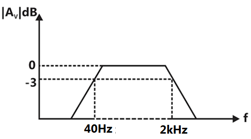
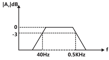
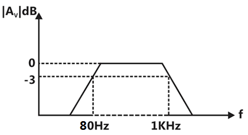
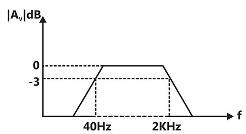
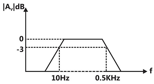
Sign in to UnlockThree identical RC-coupled transistor amplifiers are cascaded. If each of the amplifiers has a frequency response as shown in Figure, the overall frequency response is as given in
Sign in to see the solution
Log in to view the explanation, track your attempts, and keep your progress.
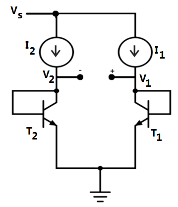
Sign in to UnlockIn the differential amplifier of Figure, if the source resistance of the current source is infinite, then the common-mode gain is

Zero
Infinite
Indeterminate

Sign in to see the solution
Log in to view the explanation, track your attempts, and keep your progress.
Sign in to UnlockAn amplifier with resistive negative feedback has two left half-plane poles in its open-loop transfer function. The amplifier
Sign in to see the solution
Log in to view the explanation, track your attempts, and keep your progress.
Sign in to UnlockFor a feedback amplifier, the open loop transfer function has three poles at, and . The low frequency open loop gain is 1000 and the feedback factor is 1. Use Bode plots to determine the phase margin of the amplifier. Is the amplifier stable?


The amplifier is stable
The amplifier is unstable
Sign in to see the solution
Log in to view the explanation, track your attempts, and keep your progress.
Sign in to UnlockNegative feedback in an amplifier
Sign in to see the solution
Log in to view the explanation, track your attempts, and keep your progress.
Sign in to UnlockCrossover distortion behaviour is characteristic of
Sign in to see the solution
Log in to view the explanation, track your attempts, and keep your progress.
Sign in to UnlockAn amplifier has an open-loop gain of 100, an input impedance of , and an output impedance of. A feedback network with a feedback factor of 0.99 is connected to the amplifier in a voltage series feedback mode. The new input and output impedances, respectively, are


and


and


and


and

Sign in to see the solution
Log in to view the explanation, track your attempts, and keep your progress.
Sign in to UnlockAn amplifier is assumed to have a single pole high frequency transfer function. The rise time of its output response to a step function input is 35nsec. The upper -3dB frequency (in MHz) for the amplifier to a sinusoidal input is approximately at
Sign in to see the solution
Log in to view the explanation, track your attempts, and keep your progress.
Sign in to UnlockThe circuit of Figure is an example of feedback of the following type
Sign in to see the solution
Log in to view the explanation, track your attempts, and keep your progress.
Sign in to UnlockIn a differential amplifier, CMRR can be improved by using an increased
Sign in to see the solution
Log in to view the explanation, track your attempts, and keep your progress.
Sign in to UnlockFrom a measurement of the rise time of the output pulse of an amplifier whose input is a small amplitude square wave, one can estimate the following parameter of the amplifier:
Sign in to see the solution
Log in to view the explanation, track your attempts, and keep your progress.
Sign in to UnlockA distorted sinusoidal has the amplitudes of the fundamental, second harmonic, third harmonic … respectively. The total harmonic distortion is


Sign in to see the solution
Log in to view the explanation, track your attempts, and keep your progress.
Sign in to UnlockThe emitter coupled pair of BJT’s gives a linear transfer relation between the differential output voltage and the differential input voltage only when the magnitude of is less times the thermal voltage, where is


Sign in to see the solution
Log in to view the explanation, track your attempts, and keep your progress.
Sign in to UnlockIn a shunt-shunt negative feedback amplifier, as compared to the basic amplifier
Sign in to see the solution
Log in to view the explanation, track your attempts, and keep your progress.
Sign in to UnlockA multistage amplifier has a low-pass response with three real poles at , and . The approximate overall bandwidth B of the amplifier will be given by


Sign in to see the solution
Log in to view the explanation, track your attempts, and keep your progress.
Sign in to UnlockA cascode amplifier stage is equivalent to
Sign in to see the solution
Log in to view the explanation, track your attempts, and keep your progress.
Sign in to UnlockNegative feedback in
(1) Voltage series configuration
(2) Current shunt configuration
(a) Increase input impedance
(b) Decrease input impedance
(c) Increases closed loop gain
(d) Leads to oscillation
Sign in to see the solution
Log in to view the explanation, track your attempts, and keep your progress.
Sign in to UnlockIn the cascade amplifier circuit shown in the figure is determine the values of , and such that the quiescent current through the transistors is 1 mA and the collector voltages are and , Take , transistor to be high and base currents to be negligible.


Sign in to see the solution
Log in to view the explanation, track your attempts, and keep your progress.
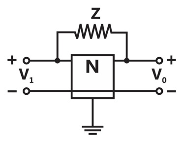
Sign in to UnlockIn the circuit shown in the given figure N is a finite gain amplifier with a gain of k, very large input impedance, and very low output impedance. The input impedance of the feedback amplifier with the feedback impedance Z connected as shown will be


Sign in to see the solution
Log in to view the explanation, track your attempts, and keep your progress.
Sign in to UnlockMatch the following
(a) Cascode amplifier
(b) Differential amplifier
(c) Darlington pair common emitter amplifier
(1) Does not provide current gain
(2) Is a wideband amplifier
(3) Has very low input impedance and very high current gain
(4) Has very high input impedance and very high current gain
(5) Provides high common mode voltage rejection
Sign in to see the solution
Log in to view the explanation, track your attempts, and keep your progress.
Sign in to UnlockTo obtain very high input and output impedances in a feedback amplifier, the mostly used is
Sign in to see the solution
Log in to view the explanation, track your attempts, and keep your progress.
Sign in to UnlockA power amplifiers delivers 50 W output at 50% efficiency. The ambient temperature is 25°C. If the maximum allowable junction temperature is, then the maximum thermal resistance that can be tolerated is _________.


Sign in to see the solution
Log in to view the explanation, track your attempts, and keep your progress.
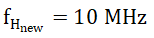
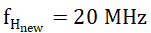
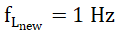
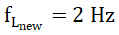
Sign in to UnlockAn amplifier has an open-loop gain of 100, and its lower-and upper-cut-off frequency of 100 Hz and 100 kHz, respectively. A feedback network with a feedback factor of 0.99 is connected to the amplifier. The new lower and upper-cut-off frequencies are at _________Hz and ________MHz.
Sign in to see the solution
Log in to view the explanation, track your attempts, and keep your progress.
Sign in to UnlockA class – A transformer coupled, transistor power amplifier is required to deliver a power output of 10 watts. The maximum power rating of the transistor should not be less than
Sign in to see the solution
Log in to view the explanation, track your attempts, and keep your progress.
Sign in to UnlockIn order to reduce the harmonic distortion in an amplifier, its dynamic range has to be increased. ( True=1,False=0)
Sign in to see the solution
Log in to view the explanation, track your attempts, and keep your progress.
Sign in to UnlockA pulse having a rise time of 40nsec is displayed on a CRO of 12MHz bandwidth. The rise time of the pulse as observed on the CRO would be approximately equal to _______ns
Sign in to see the solution
Log in to view the explanation, track your attempts, and keep your progress.
Sign in to UnlockNegative feedback in amplifiers
Sign in to see the solution
Log in to view the explanation, track your attempts, and keep your progress.
Sign in to UnlockIn a multi-stage R-C coupled amplifier the coupling capacitor
Sign in to see the solution
Log in to view the explanation, track your attempts, and keep your progress.
Sign in to UnlockThe bandwidth of an n-stage tuned amplifier, with each stage having a band width of B, is given by


Sign in to see the solution
Log in to view the explanation, track your attempts, and keep your progress.
Sign in to UnlockIn a transistor push-pull amplifier
Sign in to see the solution
Log in to view the explanation, track your attempts, and keep your progress.
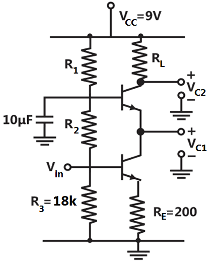
Sign in to UnlockThe transistors in the differential amplifier shown in figure are identical with and ohms at 1mA collector current. The circuit has a Common Mode Rejection Ratio (CMRR) of 100.


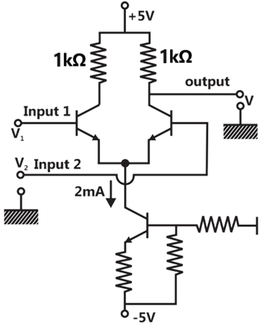
(a) What is the differential gain of the circuit?

(b) What is the common mode gain of the circuit?
(c) If DC voltage of 1010 mV and 990 mV are allied to inputs 1 and 2 respectively with reference to ground, what will be the output voltage___mV?

Sign in to see the solution
Log in to view the explanation, track your attempts, and keep your progress.
Sign in to Unlock