Electronic Devices
Semiconductor Physics
Practice questions from Semiconductor Physics.
77
Total0
Attempted0
Correct0
IncorrectWhich of the following can be used as an n-type dopant for silicon?
Select the correct option(s).
Sign in to see the solution
Log in to view the explanation, track your attempts, and keep your progress.
Sign in to UnlockThe intrinsic carrier concentration of a semiconductor is at 300 K.

If the electron and hole mobilities are and , respectively, then the intrinsic resistivity of the semiconductor (in ) at 300 K is _________.


(Charge of an electron .)

Sign in to see the solution
Log in to view the explanation, track your attempts, and keep your progress.
Sign in to UnlockThe electron mobility in a non-degenerate germanium semiconductor at 300 K is .


The electron diffusivity at 300 K (in , rounded off to the nearest integer) is _________.


(Consider the Boltzmann constant and the charge of an electron .)

Sign in to see the solution
Log in to view the explanation, track your attempts, and keep your progress.
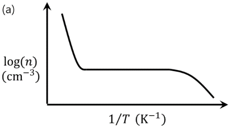
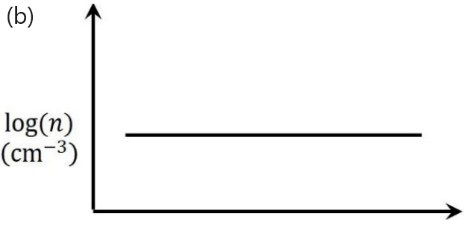
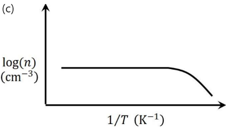
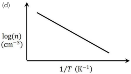
Sign in to UnlockFor non-degenerately doped n-type silicon, which one of the following plots represents the temperature (𝑇) dependence of free electron concentration (𝑛)
Sign in to see the solution
Log in to view the explanation, track your attempts, and keep your progress.
Sign in to UnlockA non-degenerate n-type semiconductor has neutral dopant atoms. Its Fermi level is located at below the conduction band and the donor energy level has a degeneracy of 2. Assuming the thermal voltage to be . The difference between and (in , rounded off to two decimal places) is __________.


Sign in to see the solution
Log in to view the explanation, track your attempts, and keep your progress.
Sign in to UnlockThe free electron concentration profile in a doped semiconductor at equilibrium is shown in the figure, where the points , and mark three different positions. Which of the following statements is/are true?


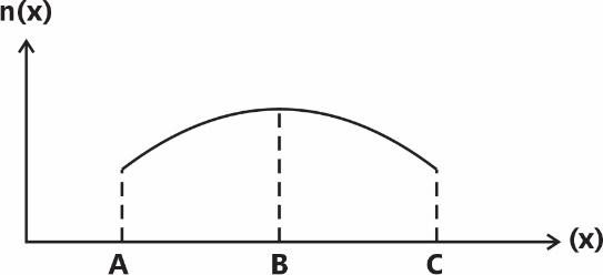
For between B and C, the electron diffusion current is directed from to .


For between B and A, the electron drift current is directed from B to A.
For between B and C, the electric field is directed from B to C.
For between B and A, the electric field is directed from to .

Sign in to see the solution
Log in to view the explanation, track your attempts, and keep your progress.
Sign in to UnlockIn a semiconductor, if the Fermi energy level lies in the conduction band, then the semiconductor is known as
degenerate -type.

degenerate -type.

non-degenerate -type.
non-degenerate -type.
Sign in to see the solution
Log in to view the explanation, track your attempts, and keep your progress.
Sign in to UnlockFor an intrinsic semiconductor at temperature , which of the following statement is true?

Sign in to see the solution
Log in to view the explanation, track your attempts, and keep your progress.
Sign in to UnlockIn an extrinsic semiconductor, the hole concentration is given to be where is the intrinsic carrier concentration of . The ratio of electron to hole mobility for equal hole and electron drift current is given as _________(rounded off to two decimal places).


Sign in to see the solution
Log in to view the explanation, track your attempts, and keep your progress.
Sign in to UnlockIn a semiconductor device, the Fermi-energy level is above the valence band energy. The effective density of states in the valence band at is . The thermal equilibrium hole concentration in silicon at is _________. (rounded off to two decimal places). Given KT at is .


Sign in to see the solution
Log in to view the explanation, track your attempts, and keep your progress.
Sign in to UnlockConsider a long rectangular bar of direct bandgap p-type semiconductor. The equilibrium hole density is and the intrinsic carrier concentration is . Electron and hole diffusion lengths are and , respectively. The left side of the bar is uniformly illuminated with a laser having photon energy greater than the bandgap of the semiconductor. Excess electron-hole pairs are generated ONLY at because of the laser. The steady state electron density at is due to laser illumination. Under these conditions and ignoring electric field, the closest approximation (among the given options) of the steady state electron density at , is _______.


Sign in to see the solution
Log in to view the explanation, track your attempts, and keep your progress.
Sign in to UnlockIn a non-degenerate bulk semiconductor with electron density , the value of , where and denote the bottom of the conduction band energy and electron Fermi level energy, respectively. Assume thermal voltage as and the intrinsic carrier concentration is . For 3 , the closest approximation of the value of , among the given options, is _________.


Sign in to see the solution
Log in to view the explanation, track your attempts, and keep your progress.
Sign in to UnlockSelect the CORRECT statement(s) regarding semiconductor devices.
Electrons and holes are of equal density in an intrinsic semiconductor at equilibrium.
Collector region is generally more heavily doped than Base region in a BJT.
Total current is spatially constant in a two terminal electronic device in dark under steady state condition.
Mobility of electrons always increases with temperature in Silicon beyond .

Sign in to see the solution
Log in to view the explanation, track your attempts, and keep your progress.
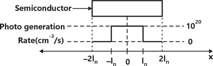
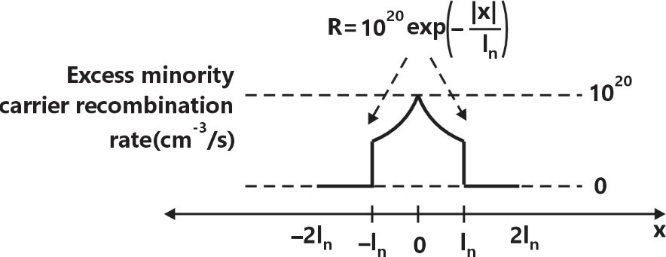
Sign in to UnlockA p-type semiconductor with zero electric field is under illumination (low level injection) in steady state condition. Excess minority carrier density is zero at , where is the diffusion length of electrons. Assume electronic charge, . The profiles of photogeneration rate of carriers and the recombination rate of excess minority carriers are shown. Under these conditions, the magnitude of the current density due to the photo-generated electrons at is __________ (rounded off to two decimal places).


Sign in to see the solution
Log in to view the explanation, track your attempts, and keep your progress.
Sign in to UnlockA bar of silicon is doped with boron concentration of and assumed to be fully ionized. It is exposed to light such that electron-hole pairs are generated throughout the volume of he bar at the rate of . If the recombination lifetime is s intrinsic carrier concentration of silicon is and assuming ionization of boron, then the approximate product of steady state electron and hole concentration due to this light exposure is


Sign in to see the solution
Log in to view the explanation, track your attempts, and keep your progress.
Sign in to UnlockThe energy band diagram of a p-type semiconductor bar of length under equilibrium condition (i.e, the Fermi energy level is constant) is shown in the figure. The valence band is sloped since doping is non-uniform along the bar. The difference between the energy levels of the valence band at the two edges of the bar is .


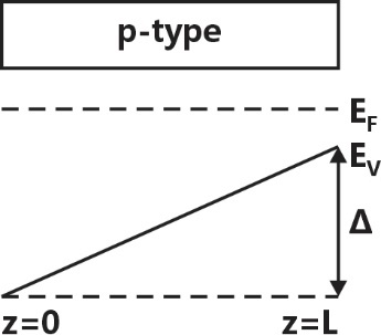
If the charge of an electron is , then the magnitude of the electric field developed inside this semiconductor bar is


Sign in to see the solution
Log in to view the explanation, track your attempts, and keep your progress.
Sign in to UnlockA silicon junction is shown in the figure. The doping in the P region is and doping in the N region is . The parameters given are


Built-in voltage

Electron charge

Vacuum permittivity

Relative permittivity of silicon

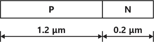
The magnitude of reverse bias voltage that would completely deplete one of the two regions ( or ) prior to the other (rounded off to one decimal place) is __________ V.


Sign in to see the solution
Log in to view the explanation, track your attempts, and keep your progress.
Sign in to UnlockA single crystal intrinsic semiconductor is at a temperature of with effective density of states for holes twice that of electrons. The thermal voltage is . The intrinsic Fermi level is shifted from mid-bandgap energy level by


Sign in to see the solution
Log in to view the explanation, track your attempts, and keep your progress.
Sign in to UnlockConsider the recombination process via bulk traps in a forward biased pn homojunction diode. The maximum recombination rate is . If the electron and the hole capture cross-section are equal, which one of the following is False?

With all other parameters unchanged, decreases if the intrinsic carrier density is reduced.
With all other parameters unchanged, increases if the thermal velocity of the carriers increases.
occurs at the edges of the depletion region in the device.
depends exponentially on the applied bias.
Sign in to see the solution
Log in to view the explanation, track your attempts, and keep your progress.
Sign in to UnlockA junction is made between p- Si with doping density and p Si with doping density


Given:
Boltzmann constant

Electronic charge . Assume 100% acceptor ionization.

At room temperature (T= 300K), the magnitude of the built-in potential (in volts. correct to two decimal places) across this junction will be ________
Sign in to see the solution
Log in to view the explanation, track your attempts, and keep your progress.
Sign in to UnlockA bar of Gallium Arsenide (GaAs) is doped with Silicon such that the Silicon atoms occupy Gallium and Arsenic in the GaAs crystal. Which one of the following statements is true?
Sign in to see the solution
Log in to view the explanation, track your attempts, and keep your progress.
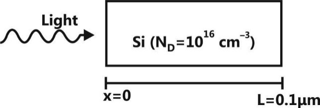
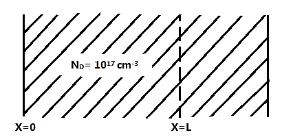
Sign in to UnlockAs shown, a uniformly doped Silicon (Si) bar of length L = 0.1 µm with a donor concentration is illuminated at x = 0 such that electron and hole pairs are generated at the rate of . Hole lifetime is , electronic charge hole diffusion coefficient and low level injection condition prevails. Assuming a linearly decaying steady state excess hole concentration that goes to 0 at x = L, the magnitude of the diffusion current density at x = L/2, in, is ____________.


Sign in to see the solution
Log in to view the explanation, track your attempts, and keep your progress.
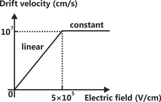
Sign in to UnlockThe dependence of drift velocity of electrons on electric field in a semiconductor is shown below. The semiconductor has a uniform electron concentration of and electronic charge . If a bias of 5 V is applied across a 1 µm region of this semiconductor, the resulting current density in this region, in , is ____________.


Sign in to see the solution
Log in to view the explanation, track your attempts, and keep your progress.
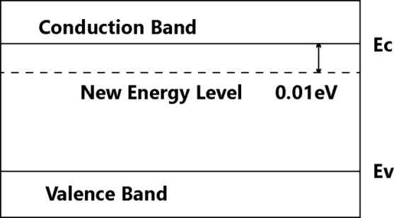
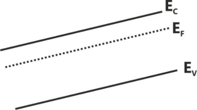
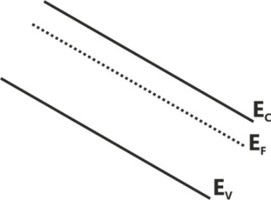
Sign in to UnlockA small percentage of impurity is added to an intrinsic semiconductor at 300 K. Which one of the following statements is true for the energy band diagram shown in the following figure?
Sign in to see the solution
Log in to view the explanation, track your attempts, and keep your progress.
Sign in to UnlockThe figure below shows the doping distribution in a p-type semiconductor in log scale.
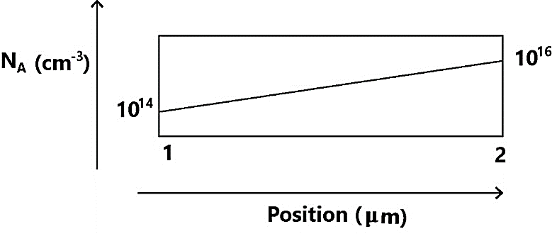
The magnitude of the electric field (in kV/cm) in the semiconductor due to non uniform doping is________
Sign in to see the solution
Log in to view the explanation, track your attempts, and keep your progress.
Sign in to UnlockConsider a silicon sample at T = 300 K, with a uniform donor density , illuminated uniformly such that the optical generation rate is throughout the sample. The incident radiation is turned off at t = 0. Assume low-level injection to be valid and ignore surface effects. The carrier lifetimes are and .


The hole concentration at t=0 and the hole concentration at t = 0.3μs, respectively, are
and


and


and


and

Sign in to see the solution
Log in to view the explanation, track your attempts, and keep your progress.
Sign in to UnlockConsider a region of silicon devoid of electrons and holes, with an ionized donor density of . The electric field at x=0 is 0 V/cm and the electric field at is 50kV/cm in the positive x direction. Assume that the electric filed is zero in the y and z directions at all points.


Given coulomb, F/cm, for silicon, the value of L in nm is ________.


Sign in to see the solution
Log in to view the explanation, track your attempts, and keep your progress.
Sign in to UnlockThe I-V characteristics of three types of diodes at the room temperature, made of semiconductors X, Y and Z, are shown in the figure. Assume that the diodes are uniformly doped and identical in all respects except their materials. If , and are the band gaps of X, Y and Z, respectively, the


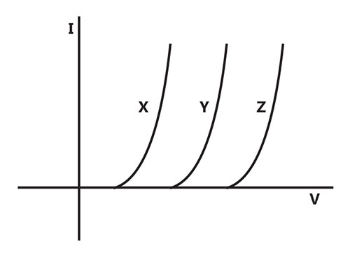


No relationship among these band gaps exists.
Sign in to see the solution
Log in to view the explanation, track your attempts, and keep your progress.
Sign in to UnlockA silicon sample is uniformly doped with donor type impurities with a concentration of . The electron and hole mobilities in the sample are and respectively. Assume complete ionization of impurities. The charge of an electron is . The resistivity of the sample (in Ω-cm) is ____________.


Sign in to see the solution
Log in to view the explanation, track your attempts, and keep your progress.
Sign in to UnlockAn n-type silicon sample is uniformly illuminated with light which generates electron-hole pairs per per second. The minority carrier lifetime in the sample is 1 µs. In the steady state, the hole concentration in the sample is approximately , where x is an integer. The value of x is ___.


Sign in to see the solution
Log in to view the explanation, track your attempts, and keep your progress.
Sign in to UnlockA piece of silicon is doped uniformly with phosphorous with a doping concentration of . The expected value of mobility versus doping concentration for silicon assuming full dopant ionization is shown below. The charge of an electron is . The conductivity (in S ) of the silicon sample at 300 K is _______.


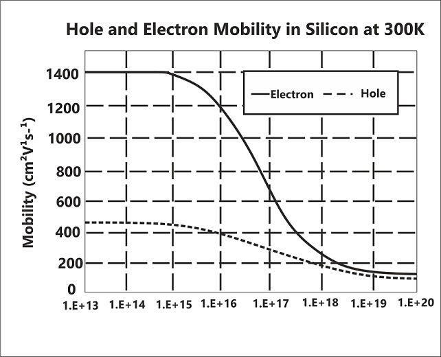
Sign in to see the solution
Log in to view the explanation, track your attempts, and keep your progress.
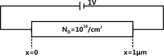
Sign in to UnlockA dc voltage of 10 V is applied across an n-type silicon bar having a rectangular cross-section and a length of 1 cm as shown in figure. The donor doping concentration and the mobility of electrons are and , respectively. The average time (in µs) taken by the electrons to move from one end of the bar to other end is ________.


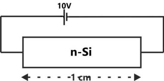
Sign in to see the solution
Log in to view the explanation, track your attempts, and keep your progress.
Sign in to UnlockThe energy band diagram and the electron density profile n(x) in a semiconductor are shown in the figures. Assume that n(x) =, with α=0.1 V/cm and x expressed in cm. Given , and . The electron current density (in ) at


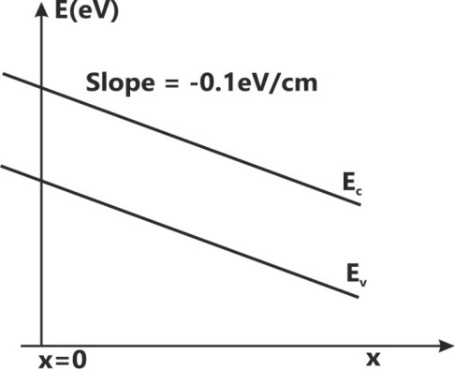


0

Sign in to see the solution
Log in to view the explanation, track your attempts, and keep your progress.
Sign in to UnlockA silicon bar is doped with donor impurities. Given the intrinsic carrier concentration of silicon at T = 300 K is. Assuming complete impurity ionization, the equilibrium electron and hole concentrations are


Sign in to see the solution
Log in to view the explanation, track your attempts, and keep your progress.
Sign in to UnlockAssume electronic charge , and electron mobility . If the concentration gradient of electrons injected into a P-type silicon sample is , the magnitude of electron diffusion current density (in ) is _________.


Sign in to see the solution
Log in to view the explanation, track your attempts, and keep your progress.
Sign in to UnlockA thin P-type silicon sample is uniformly illuminated with light which generates excess carriers. The recombination rate is directly proportional to
Sign in to see the solution
Log in to view the explanation, track your attempts, and keep your progress.
Sign in to UnlockAt T = 300 K, the hole mobility of a semiconductor and. The hole diffusion constant in is ________.


Sign in to see the solution
Log in to view the explanation, track your attempts, and keep your progress.
Sign in to UnlockIn the figure, ln is plotted as a function of 1/T, where is the intrinsic resistivity of silicon, T is the temperature, and the plot is almost linear.


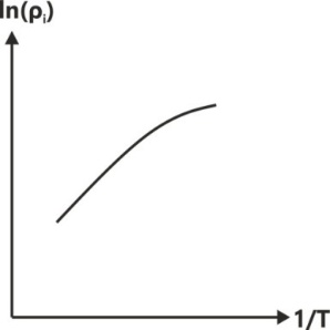
The slope of the line can be used to estimate
Band gap energy of silicon ()

Sum of electron and hole mobility in silicon ()

Reciprocal of the sum of electron and hole mobility in silicon ()-1
Intrinsic carrier concentration of silicon ()

Sign in to see the solution
Log in to view the explanation, track your attempts, and keep your progress.
Sign in to UnlockConsider a silicon sample doped with donor atoms. Assume that the intrinsic carrier concentration.


If the sample is additionally doped with acceptor atoms, the approximate number of in the sample, at T=300 K, will be ______.


Sign in to see the solution
Log in to view the explanation, track your attempts, and keep your progress.
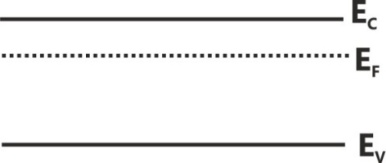
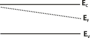
Sign in to UnlockAn N-type semiconductor having uniform doping is biased as shown in the figure.
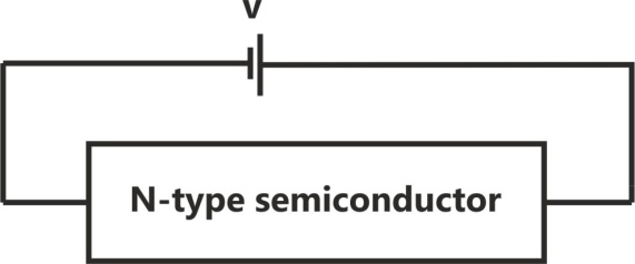
If is the lowest energy level of the conduction band, is the highest energy level of the valence band and is the Fermi level, which one of the following represents the energy band diagram for the biased N-type semiconductor?
Sign in to see the solution
Log in to view the explanation, track your attempts, and keep your progress.
Sign in to UnlockDrift current in semiconductors depends upon
Sign in to see the solution
Log in to view the explanation, track your attempts, and keep your progress.
Sign in to UnlockThe silicon sample with unit cross-sectional area shown below is in thermal equilibrium. The following information is given: T=300K, electronic charge= , thermal voltage=26mV and electron mobility=


The magnitude of the electric field at is

Sign in to see the solution
Log in to view the explanation, track your attempts, and keep your progress.
Sign in to UnlockThe silicon sample with unit cross-sectional area shown below is in thermal equilibrium. The following information is given: T=300K, electronic charge= , thermal voltage=26mV and electron mobility=
The magnitude of the electron drift current density at is


Sign in to see the solution
Log in to view the explanation, track your attempts, and keep your progress.
Sign in to UnlockIn an n-type silicon crystal at room temperature, which of the following can have a concentration of?

Sign in to see the solution
Log in to view the explanation, track your attempts, and keep your progress.
Sign in to UnlockThe ratio of the mobility to the diffusion coefficient in a semiconductor has the units


Sign in to see the solution
Log in to view the explanation, track your attempts, and keep your progress.
Sign in to UnlockWhich of the following is true?
A silicon wafer heavily doped with boron is a substrate

A silicon wafer lightly doped with boron is a substrate
A silicon wafer heavily doped with arsenic is a substrate
A silicon wafer lightly doped with arsenic is a substrate
Sign in to see the solution
Log in to view the explanation, track your attempts, and keep your progress.
Sign in to UnlockSilicon is doped with boron to a concentration of atom/. Assume the intrinsic carrier concentration of silicon to be and the value of to be 25mV at 300 K. Compared to un-doped silicon, the Fermi level of doped silicon


Sign in to see the solution
Log in to view the explanation, track your attempts, and keep your progress.
Sign in to UnlockThe electron and hole concentrations in an intrinsic semiconductor are per at 300 K. Now, if acceptor impurities are introduced with a concentration of per (where ), the electron concentration per at 300 K will be


Sign in to see the solution
Log in to view the explanation, track your attempts, and keep your progress.
Sign in to UnlockThe concentration of minority carriers in an extrinsic semiconductor under equilibrium is:
Sign in to see the solution
Log in to view the explanation, track your attempts, and keep your progress.
Sign in to UnlockUnder low level injection assumption, the injected minority carrier current for an extrinsic semiconductor is essentially the
Sign in to see the solution
Log in to view the explanation, track your attempts, and keep your progress.
Sign in to UnlockThe majority carriers in an n-type semiconductor have an average drift velocity v in a direction perpendicular to a uniform magnetic field B. the electric field E induced due to Hall effect acts in the direction
Sign in to see the solution
Log in to view the explanation, track your attempts, and keep your progress.
Sign in to UnlockA heavily doped n-type semiconductor has the following data:
Hole-electron mobility ratio : 0.4
Doping concentration :

Intrinsic concentration :

The ratio of conductance of the n-type semiconductor to that of the intrinsic semiconductor of same material and at same temperature is given by
Sign in to see the solution
Log in to view the explanation, track your attempts, and keep your progress.
Sign in to UnlockThe band gap of silicon at room temperature is:
Sign in to see the solution
Log in to view the explanation, track your attempts, and keep your progress.
Sign in to UnlockThe primary reason for the widespread use of silicon in semiconductor device technology is
Abundance of silicon on the surface of the Earth.
Larger bandgap of silicon in comparison to Germanium
Favorable properties of silicon-dioxide

Lower melting point
Sign in to see the solution
Log in to view the explanation, track your attempts, and keep your progress.
Sign in to UnlockA silicon sample A is doped with of Boron. Another sample B of identical dimensions is doped with of Phosphorus. The ratio of electron to hole mobility is 3. The ratio of conductivity of the sample A to B is

3


Sign in to see the solution
Log in to view the explanation, track your attempts, and keep your progress.
Sign in to UnlockThe impurity commonly used for realizing the base region of a silicon n-p-n transistor is
Sign in to see the solution
Log in to view the explanation, track your attempts, and keep your progress.
Sign in to UnlockThe resistivity of a uniformly doped n-type silicon sample is 0.5Ω-cm. If the electron mobility is and the charge of an electron is Coulomb, the donor impurity concentration in the sample is


Sign in to see the solution
Log in to view the explanation, track your attempts, and keep your progress.
Sign in to Unlockn-type silicon is obtained by doping silicon with
Sign in to see the solution
Log in to view the explanation, track your attempts, and keep your progress.
Sign in to UnlockThe bandgap of silicon at 300 K is
Sign in to see the solution
Log in to view the explanation, track your attempts, and keep your progress.
Sign in to UnlockThe intrinsic carrier concentration of silicon sample of 300 K is . If after doping, the number of majority carriers is , the minority carrier density is


Sign in to see the solution
Log in to view the explanation, track your attempts, and keep your progress.
Sign in to UnlockAn n-type silicon bar 0.1 cm long and 100 in cross-sectional area has a majority carrier concentration of and the carrier mobility is at 300K. if the charge of an electron is coulomb, then the resistance of the bar is


ohm

ohm

ohm

ohm

Sign in to see the solution
Log in to view the explanation, track your attempts, and keep your progress.
Sign in to UnlockThe electron concentration in a sample of uniformly doped n-type silicon at 300 K varies linearly from at x = 0 to 6x at x = 2μm. Assume a situation that electrons are supplied to keep this concentration gradient constant with time. If electronic charge is coulombs and the diffusion constant , the current density in the silicon, if no electric field is present, is


Zero


Sign in to see the solution
Log in to view the explanation, track your attempts, and keep your progress.
Sign in to UnlockThe electron and hole concentrations in a intrinsic semiconductor are and respectively. When doped with a p-type material, these change to n and p, respectively. Then


Sign in to see the solution
Log in to view the explanation, track your attempts, and keep your progress.
Sign in to UnlockA long specimen of p-type semiconductor material
Sign in to see the solution
Log in to view the explanation, track your attempts, and keep your progress.
Sign in to UnlockThe units of are

V
J

Sign in to see the solution
Log in to view the explanation, track your attempts, and keep your progress.
Sign in to UnlockThe intrinsic carrier density at 300 K is , in silicon. For n-type silicon doped to , the equilibrium electron and hole densities are

,


,


,


,
Sign in to see the solution
Log in to view the explanation, track your attempts, and keep your progress.
Sign in to UnlockAn n-type silicon bar is doped uniformly by phosphorus atoms to a concentration. The bar has cross- section of and length of 10 cm. It is illuminated uniformly for region as shown in the figure is assume optical generation rate Electron-Hole pairs per per second, for this case. The hole lifetime and electron lifetime are equal, and equal to .


Evaluate the hole and electron diffusion currents at .

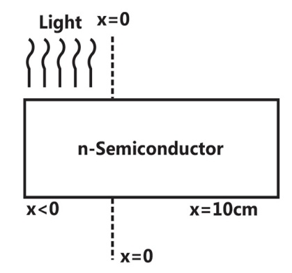
Following expressions and data can be used in this evaluation


Where ;


coloumbs ;


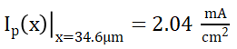
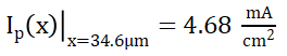
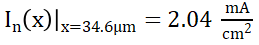
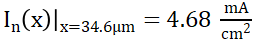
Sign in to see the solution
Log in to view the explanation, track your attempts, and keep your progress.
Sign in to UnlockThe probability that an electron in a metal occupies the Fermi-level at any temperature

Sign in to see the solution
Log in to view the explanation, track your attempts, and keep your progress.
Sign in to UnlockThe drift velocity of electrons, in silicon
Sign in to see the solution
Log in to view the explanation, track your attempts, and keep your progress.
Sign in to UnlockIn a P type silicon sample, the hole concentration is . If the intrinsic carrier concentration is , the electron concentration is

Zero


Sign in to see the solution
Log in to view the explanation, track your attempts, and keep your progress.
Sign in to UnlockIn an extrinsic semiconductor if
(A) The resistivity decreases
(B) The temperature coefficient of resistivity is negative
(C) The photo conductivity is low
(1) The doping concentration is low
(2) The length of the semiconductor is reduced
(3) The band gap is high
(4) The area of cross-section of the semiconductor is increased
(5) The doping concentration is increased
Sign in to see the solution
Log in to view the explanation, track your attempts, and keep your progress.
Sign in to UnlockA small concentration of minority carriers is injected into a homogeneous semiconductor crystal at one point. An electric field of 10 V/cm is applied across the crystal and this moves the minority carriers a distance of 1 cm in sec. The mobility (in /volt.sec) will be


Sign in to see the solution
Log in to view the explanation, track your attempts, and keep your progress.
Sign in to UnlockA p-type silicon sample has a higher conductivity compared to an n-type sample having the same dopant concentration. (True=1,False=0)
Sign in to see the solution
Log in to view the explanation, track your attempts, and keep your progress.
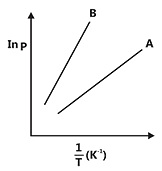
Sign in to UnlockConsider the semiconductors A and B. The figure shows variation of lnρ with 1/T, where ρ is resistivity and T the temperature, for the two semiconductors. Choose the correct statement.
Sign in to see the solution
Log in to view the explanation, track your attempts, and keep your progress.
Sign in to UnlockA semiconductor is irradiated with light such that carriers are uniformly generated throughout its volume. The semiconductor is n-type with per . If the excess electron concentration in the steady state is per and if [minority carrier life time] the generation rate due to irradiation


Is pairs//s

Is pairs//s

Is pairs//s

Cannot be determined as the given data is insufficient
Sign in to see the solution
Log in to view the explanation, track your attempts, and keep your progress.
Sign in to UnlockA silicon sample is uniformly doped with phosphorous atoms/ and boron atoms/.If all the dopants are fully ionized, the material is


n-type with carrier concentration of

p-type with carrier concentration of
p-type with carrier concentration of

n-type with carrier concentration of 2x
Sign in to see the solution
Log in to view the explanation, track your attempts, and keep your progress.
Sign in to UnlockAn n-type silicon sample, having electron mobility = twice the hole mobility , is subjected to a steady illumination such that the electron concentration doubles from its thermal equilibrium value. As a result, the conductivity of the sample increases by a factor of


Sign in to see the solution
Log in to view the explanation, track your attempts, and keep your progress.
Sign in to Unlock