Digital Electronics
Logic Family
Practice questions from Logic Family.
40
Total0
Attempted0
Correct0
IncorrectSelect the correct statement(s) regarding CMOS implementation of NOT gates.
Noise Margin High is always equal to the Noise Margin Low , irrespective of the sizing of transistors


Dynamic power consumption during switching is zero.
For a logical high input under steady state, the nMOSFET is in the linear regime of operation.
Mobility of electrons never influences the switching speed of the NOT gate.
Sign in to see the solution
Log in to view the explanation, track your attempts, and keep your progress.
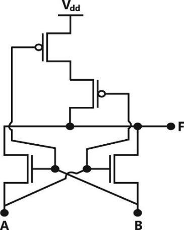
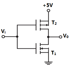
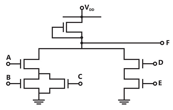
Sign in to UnlockIn the circuit shown, A and B are the inputs and F is the output. What is the functionality of the circuit?
Sign in to see the solution
Log in to view the explanation, track your attempts, and keep your progress.
Sign in to UnlockIn the circuit shown, what are the values of F for EN=0 and EN=1, respectively?
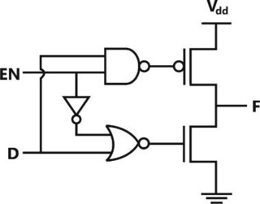
0 and 1
Hi-Z and D
0 and D
Hi-Z and

Sign in to see the solution
Log in to view the explanation, track your attempts, and keep your progress.
Sign in to UnlockA standard CMOS inverter is designed with equal rise and fall times. If the width of the pMOS transistor in the inverter is increased, what would be the effect on the LOW noise marginand the HIGH noise margin?


decreases andincreases

Bothandincrease
No change in the noise margin
increases anddecreases
Sign in to see the solution
Log in to view the explanation, track your attempts, and keep your progress.
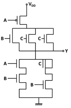
Sign in to UnlockThe logic function realized by the given circuit is


Sign in to see the solution
Log in to view the explanation, track your attempts, and keep your progress.
Sign in to UnlockFor the circuit shown in the figure, P and Q are the inputs and Y is the output.
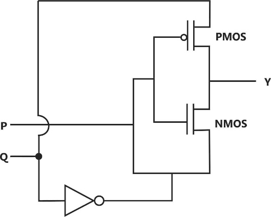
The logic implemented by the circuit is
Sign in to see the solution
Log in to view the explanation, track your attempts, and keep your progress.
Sign in to UnlockWhat is the voltage in the following circuit?

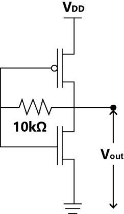
0 V

Switching threshold of inverter

Sign in to see the solution
Log in to view the explanation, track your attempts, and keep your progress.
Sign in to UnlockTransistor geometries in a CMOS inverter have been adjusted to meet the requirement for worst case charge and discharge times for driving a load capacitor C. This design is to be converted to that of a NOR circuit in the same technology, so that its worst case charge and discharge times while driving the same capacitor are similar. The channel lengths of all transistors are to be kept unchanged. Which one of the following statements is correct?
Sign in to see the solution
Log in to view the explanation, track your attempts, and keep your progress.
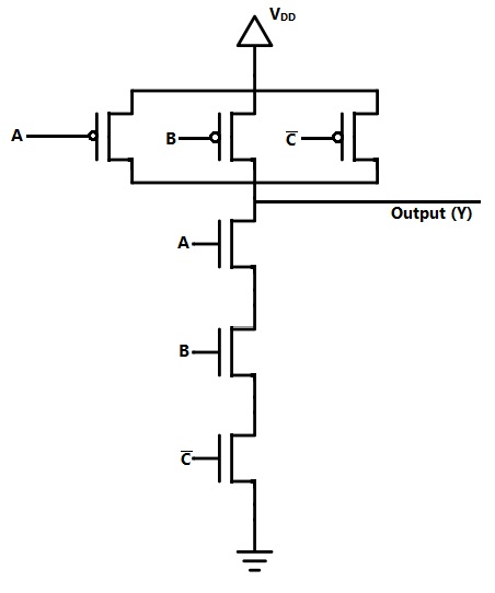
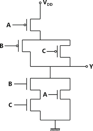
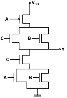
Sign in to UnlockThe logic functionality realized by the circuit shown below is
Sign in to see the solution
Log in to view the explanation, track your attempts, and keep your progress.
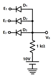
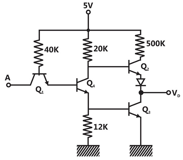
Sign in to UnlockIn the circuit shown, diodes , and are ideal, and the inputs , and are “0 V” for logic ‘0’ and “10 V” for logic ‘1’. What logic gate does the circuit represent?


Sign in to see the solution
Log in to view the explanation, track your attempts, and keep your progress.
Sign in to UnlockThe output (Y) of the circuit shown in the figure is


Sign in to see the solution
Log in to view the explanation, track your attempts, and keep your progress.
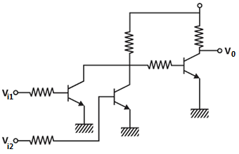
Sign in to UnlockIn the circuit shown below has negligible collector-to-emitter saturation voltage and the diode drops negligible voltage across it under forward bias. If as logic 1, then the Boolean expression for Z is


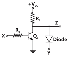
X Y


Sign in to see the solution
Log in to view the explanation, track your attempts, and keep your progress.
Sign in to UnlockIn the circuit shown


Sign in to see the solution
Log in to view the explanation, track your attempts, and keep your progress.
Sign in to UnlockThe full forms of the abbreviations TTL and CMOS in reference to logic families are
Sign in to see the solution
Log in to view the explanation, track your attempts, and keep your progress.
Sign in to UnlockThe logic function implemented by the following circuit at the terminal OUT is
Sign in to see the solution
Log in to view the explanation, track your attempts, and keep your progress.
Sign in to UnlockThe circuit diagram of a standard TTL NOT gate is shown in the figure. When , the modes of operation of the transistors will be

: reverse active;

: normal active;

: saturation;

: cut-off

: reverse active,
: saturation;
: saturation;
: cut-off
: normal active;
: cut-off,
: cut-off,
: saturation
: saturation;
: saturation;
: saturation;
: normal active
Sign in to see the solution
Log in to view the explanation, track your attempts, and keep your progress.
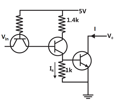
Sign in to UnlockThe transistors used in a portion of the TTL gate shown in figure have . The base-emitter voltage of is 0.7V for a transistor in active region and 0.75V for a transistor in saturation. If the sink current I=1mA and the output is at logic 0, then the current will be equal to


Sign in to see the solution
Log in to view the explanation, track your attempts, and keep your progress.
Sign in to UnlockFigure shows the internal schematic of a TTL AND-OR-Invert (AOI) gate. For the inputs shown in Figure, the output Y is
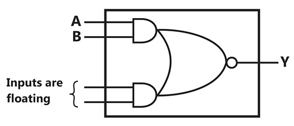
0
1
AB

Sign in to see the solution
Log in to view the explanation, track your attempts, and keep your progress.
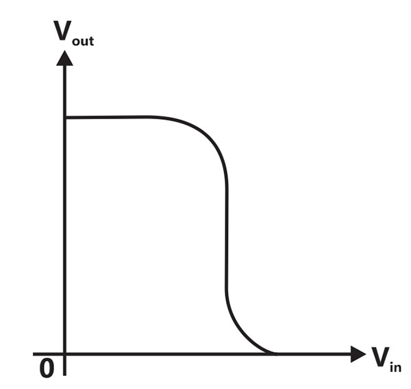
Sign in to UnlockFigure is the voltage transfer characteristic of
Sign in to see the solution
Log in to view the explanation, track your attempts, and keep your progress.
Sign in to UnlockThe output of the 74 series of TTL gates is taken from a BJT in
Sign in to see the solution
Log in to view the explanation, track your attempts, and keep your progress.
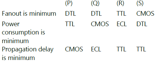
Sign in to UnlockThe DTL, TTL, ECL and CMOS families of digital ICs are compared in the following 4 columns
The correct column is
Sign in to see the solution
Log in to view the explanation, track your attempts, and keep your progress.
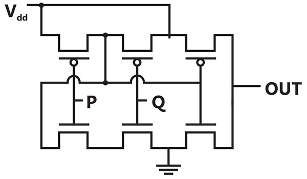
Sign in to UnlockConsider the following statements in connection with the CMOS inverter in figure where both the MOSFETs are of enhancement type and both have a threshold voltage of 2V.
Statement 1: conducts when


Statement 2: is always in saturation when

Which of the following is correct?
Sign in to see the solution
Log in to view the explanation, track your attempts, and keep your progress.
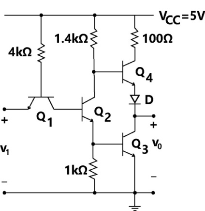
Sign in to UnlockEach transistor in Figure has dc current gain , cut-in voltage and . The output voltage for in saturation can be as high as 0.2 V. Assume 0.7 V drop across a conducting p-n junction. Determine


(a) The minimum level necessary to keep saturation.

(b) The maximum permissible value for the resistance .

(c) The worst-case high input (logic 1) and the worst-case low input (logic 0) for which will be either in saturation or in cut off.
(a)
(a)
(b)

(c)
Sign in to see the solution
Log in to view the explanation, track your attempts, and keep your progress.
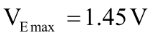
Sign in to UnlockIn Figure, the LED
Emits light when both and are closed.


Emits light when both and are open.
Emits light when only or is closed.
Does not emits light, irrespective of the switch positions.
Sign in to see the solution
Log in to view the explanation, track your attempts, and keep your progress.
Sign in to UnlockA Darlington emitter-follower circuit is sometimes used in the output stage of a TTL gate in order to
Increase its

Reduces its

Increases its speed of operation
Reduce power dissipation
Sign in to see the solution
Log in to view the explanation, track your attempts, and keep your progress.
Sign in to UnlockCommercially available ECL gates use two ground lines and one negative supply in order to
Sign in to see the solution
Log in to view the explanation, track your attempts, and keep your progress.
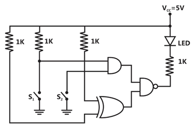
Sign in to UnlockIn the CMOS inverter circuit shown in Figure, the input makes a transition from to . Determine the high-to-low propagation delay time (μsec). when it is driving capacitance load of 20pF. Device data:


NMOS: ; , ,


PMOS: ; , .


Neglect body effect.
Sign in to see the solution
Log in to view the explanation, track your attempts, and keep your progress.
Sign in to UnlockThe noise margin of a TTL gate is about
Sign in to see the solution
Log in to view the explanation, track your attempts, and keep your progress.
Sign in to UnlockThe threshold voltage for each transistor in Figure is 2V. For this circuit to work as an inverter must take the values
Sign in to see the solution
Log in to view the explanation, track your attempts, and keep your progress.
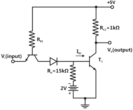
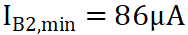
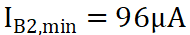
Sign in to UnlockFor the TTL circuit shown in Figure, find the current (μA)through the collector of transistor When .


Assume, and , the of in its inverse active mode is 0.01.]


Sign in to see the solution
Log in to view the explanation, track your attempts, and keep your progress.
Sign in to UnlockIn standard TTL, the ‘totem pole’ stage refers to
Sign in to see the solution
Log in to view the explanation, track your attempts, and keep your progress.
Sign in to UnlockThe inverter 74 ALSO4 has the following specifications
,

, ,


,

The fan out based on the above will be
Sign in to see the solution
Log in to view the explanation, track your attempts, and keep your progress.
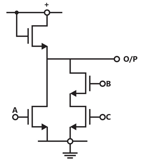
Sign in to UnlockFor the NMOS logic gate shown in the figure is the logic function implemented is


Sign in to see the solution
Log in to view the explanation, track your attempts, and keep your progress.
Sign in to UnlockFind static Noise-Margins for a BJT inverter shown in the figure is Transistor used is an n-p-n type with specifications as follows
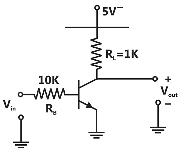


Also

and

Supply.

Sign in to see the solution
Log in to view the explanation, track your attempts, and keep your progress.
Sign in to UnlockSchottky clamping is resorted in TTL gates
Sign in to see the solution
Log in to view the explanation, track your attempts, and keep your progress.
Sign in to UnlockFor a TTL gate, match the following
(A)

(B)

(C)

(1) 2.4 volts
(2) 1.5 volts
(3) 0.4 volts
(4) 2.0 volts
(5) 0.8 volts
Sign in to see the solution
Log in to view the explanation, track your attempts, and keep your progress.
Sign in to UnlockIn the output stage of a standard TTL, have a diode between the emitter of the pull-up transistor and the collector of the pull-down transistor. The purpose of this diode is to isolate the output node from the power supply ( True=1, False=0)

Sign in to see the solution
Log in to view the explanation, track your attempts, and keep your progress.
Sign in to UnlockThe figure shows the circuit of a gate in the Resistor Transistor Logic (RTL) family. The circuit represents a
Sign in to see the solution
Log in to view the explanation, track your attempts, and keep your progress.
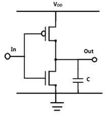
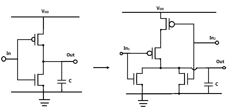
Sign in to UnlockThe CMOS equivalent of the following NMOS gate (in figure) is ____________ (draw the circuit).
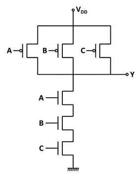
Sign in to see the solution
Log in to view the explanation, track your attempts, and keep your progress.
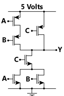
Sign in to UnlockIn figure, the Boolean expression for the output in terms of inputs A, B and C when the clock ‘CK’ is high, is given by
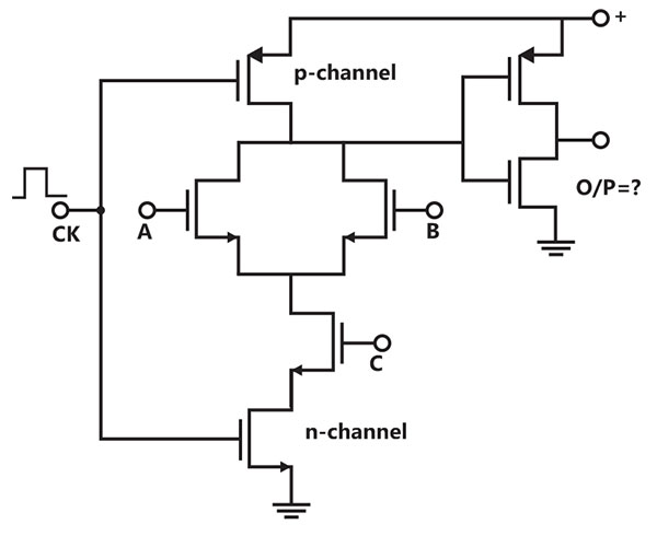
Sign in to see the solution
Log in to view the explanation, track your attempts, and keep your progress.
Sign in to Unlock