Analog Electronics
Diode and Its Applications
Practice questions from Diode and Its Applications.
66
Total0
Attempted0
Correct0
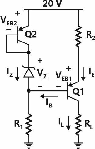
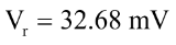
IncorrectIn the circuit shown, the identical transistors Q1 and Q2 are biased in the active region with . The Zener diode is in the breakdown region with and .


If and , then the values of and (in , rounded off to one decimal place) are __________, respectively.


Sign in to see the solution
Log in to view the explanation, track your attempts, and keep your progress.
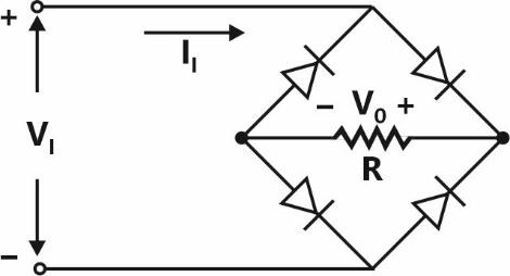
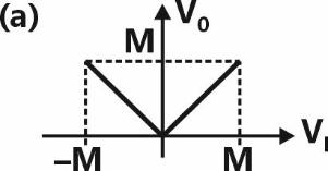
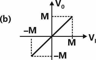
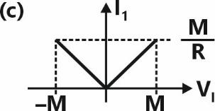
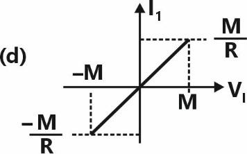
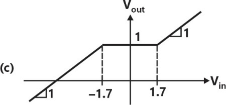
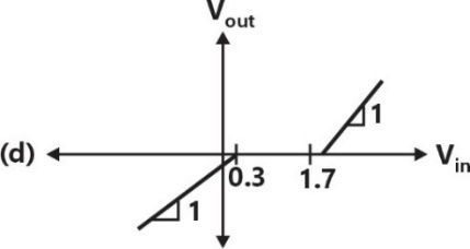
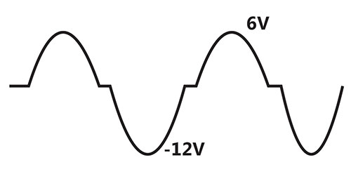
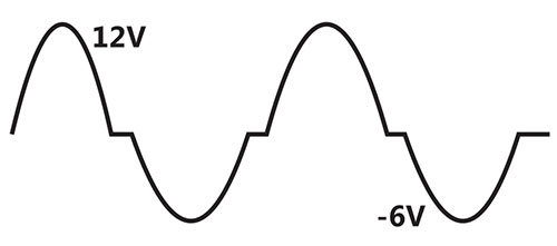
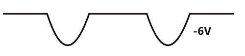
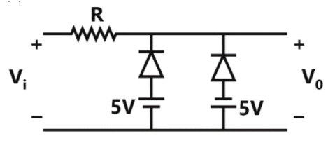
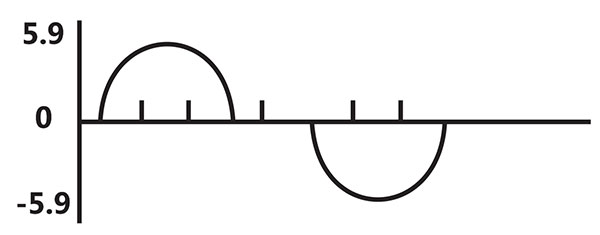
Sign in to UnlockAll the diodes in the circuit given below are ideal.
Which of the following plots is/are correct when (in Volts) is swept from - M to M?

Sign in to see the solution
Log in to view the explanation, track your attempts, and keep your progress.
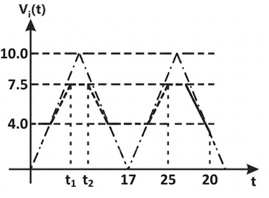
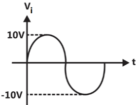
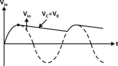
Sign in to UnlockThe diode in the circuit shown below is ideal. The input voltage (in Volts) is given by , where time t is in seconds.

The time duration (in ms, rounded off to two decimal places) for which the diode is forward biased during one period of the input is ________ .
Sign in to see the solution
Log in to view the explanation, track your attempts, and keep your progress.
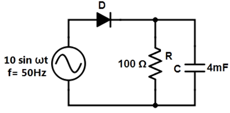
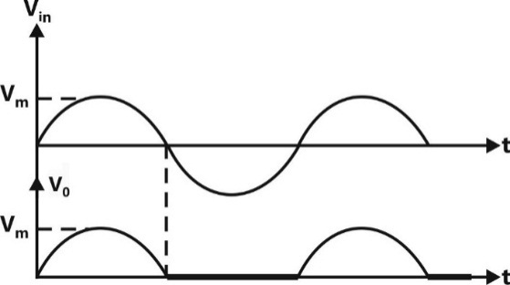
Sign in to UnlockIn the circuit shown, the step-down transformer and the diodes are ideal. The diodes have no voltage drop in forward biased condition. If the input voltage (in Volts) is and the average value of load voltage (in Volts) is , the value of is ________.


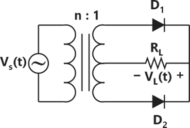
Sign in to see the solution
Log in to view the explanation, track your attempts, and keep your progress.
Sign in to UnlockAs shown in the circuit, the initial voltage across the capacitor is , with the switch being open. The switch is then closed at . The total energy dissipated in the ideal Zener diode after the switch is closed (in , rounded off to three decimal places) is ________.


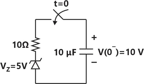
Sign in to see the solution
Log in to view the explanation, track your attempts, and keep your progress.
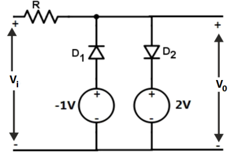
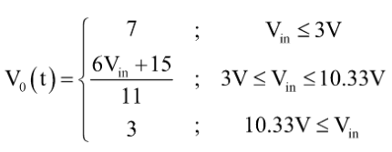
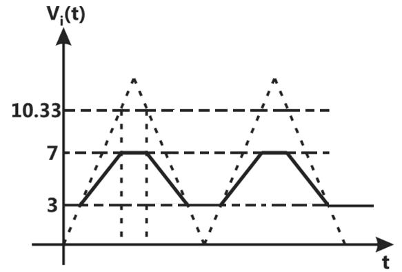
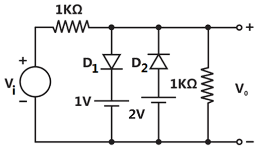
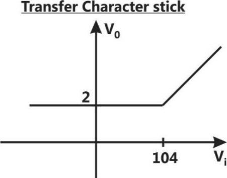
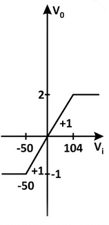
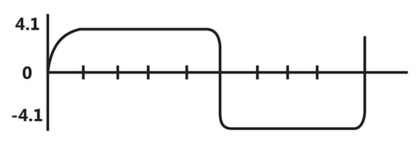
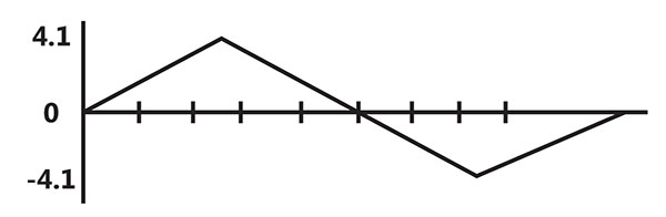
Sign in to UnlockIn the circuit shown below, and are silicon diodes with cut-in voltage of . and are input and output voltages in volts. The transfer characteristic is


Sign in to see the solution
Log in to view the explanation, track your attempts, and keep your progress.
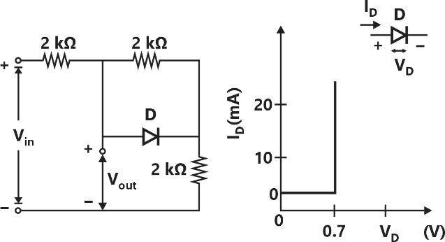
Sign in to UnlockA circuit and the characteristics of the diode (D) in it are shown. The ratio of the minimum to the maximum small signal voltage gain is __________ (rounded off to two decimal places).

Sign in to see the solution
Log in to view the explanation, track your attempts, and keep your progress.
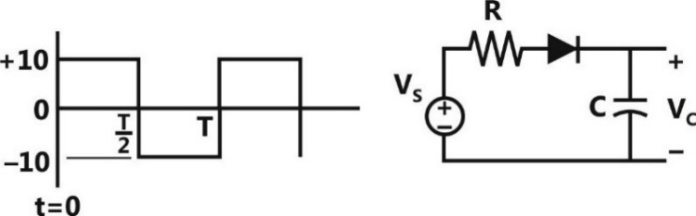
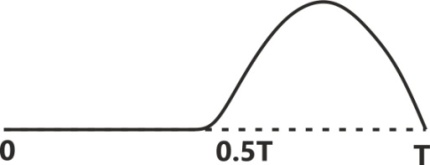
Sign in to UnlockAn symmetrical periodic pulse train of amplitude with on-time and off-time is applied to the circuit shown in the figure. The diode is ideal.


The difference between the maximum voltage and minimum voltage of the output waveform (in integer) is __________ V.

Sign in to see the solution
Log in to view the explanation, track your attempts, and keep your progress.
Sign in to UnlockIn the circuit shown below, all the components are ideal and the input voltage is sinusoidal. The magnitude of the steady-state output (rounded off to two decimal places) is _________V.

Sign in to see the solution
Log in to view the explanation, track your attempts, and keep your progress.
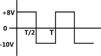
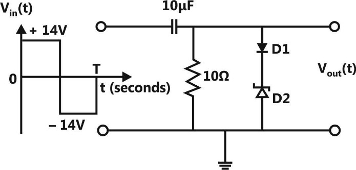
Sign in to UnlockIn the circuit shown,is a square wave of period T with maximum and minimum values of 8V and -10V respectively. Assume that the diode is ideal and


The average value ofis ______ Volts (rounded off to 1 decimal place)

Sign in to see the solution
Log in to view the explanation, track your attempts, and keep your progress.
Sign in to UnlockIn the circuit shown, the breakdown voltage and the maximum current of the Zener diode are 20V and 60mA respectively. The values ofand are 200Ω and 1kΩ respectively. What is the range ofthat will maintain the Zener diode in the ‘ON’ state?


Sign in to see the solution
Log in to view the explanation, track your attempts, and keep your progress.
Sign in to UnlockIn the circuit shown, is a 10 V square wave of period, with and The capacitor is initially uncharged at t=0, and the diode is assumed to be ideal. The voltage across the capacitor at 3 ms is equal to __________ volts (rounded off to one decimal place).


Sign in to see the solution
Log in to view the explanation, track your attempts, and keep your progress.
Sign in to UnlockA DC current of flows through the circuit shown. The diode in the circuit is forward biased and it has an ideality factor of one. At the quiescent point, the diode has a junction capacitance of 0.5nF. Its neutral region resistances can be neglected. Assume that the room temperature thermal equivalent voltage is 26mV.

For, the amplitude of the small-signal component of diode current (in, correct to one decimal place) is _______


Sign in to see the solution
Log in to view the explanation, track your attempts, and keep your progress.
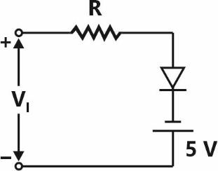
Sign in to UnlockThe circuit shown in the figure is used to provide regulated voltage (5V) across the resistor. Assume that the Zener diode has a constant reverse breakdown voltage for a current range, starting from a minimum required Zener current, its maximum allowable current. The input voltage may vary by 5% from its nominal value of 6V. The resistance of the diode in the breakdown region is negligible.


The value of R and the minimum required power dissipation rating of the diode, respectively, are
and 10mW

and 40mW

and 10Mw
and 10mW
Sign in to see the solution
Log in to view the explanation, track your attempts, and keep your progress.
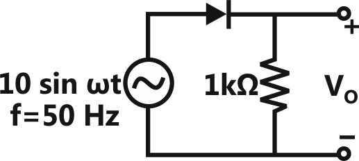
Sign in to UnlockThe output of the diode circuit shown in the figure is connected to an averaging DC voltmeter. The reading on the DC voltmeter in Volts, neglecting the voltage drop across the diode, is _________.
Sign in to see the solution
Log in to view the explanation, track your attempts, and keep your progress.
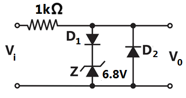
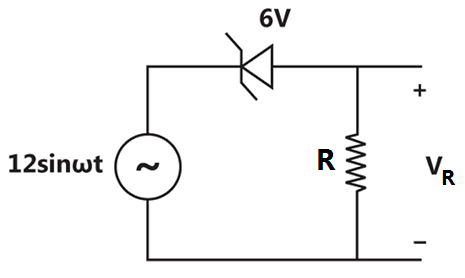
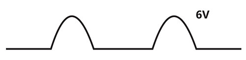
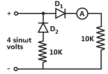
Sign in to UnlockIn the figure, D1 is a real silicon pn junction diode with a drop of 0.7 V under forward bias condition and D2 is a Zener diode with breakdown voltage of – 6.8 V. The input is a periodic square wave of period T, whose one period is shown in the figure.

Assuming , where is the time constant of the circuit, the maximum and minimum values of the output waveform are respectively.


Sign in to see the solution
Log in to view the explanation, track your attempts, and keep your progress.
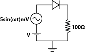
Sign in to UnlockAn AC voltage source V = 10 sin(t) volts is applied to the following network. Assume that , and , and that the diode is ideal.


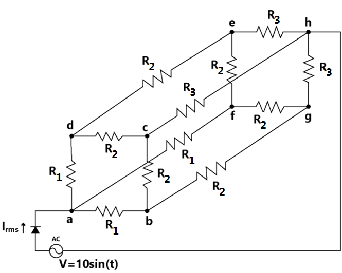
RMS current (in mA) through the diode is______________.

Sign in to see the solution
Log in to view the explanation, track your attempts, and keep your progress.
Sign in to UnlockAssume that the diode in the figure has , but is otherwise ideal.

The magnitude of the current (in mA) is equal to ____.

Sign in to see the solution
Log in to view the explanation, track your attempts, and keep your progress.
Sign in to UnlockThe switch S in the circuit shown has been closed for a long time. It is opened at time t=0 and remains open after that. Assume that the diode has zero reverse current and zero forward voltage drop.
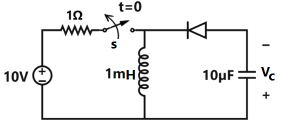
The steady state magnitude of the capacitor voltage (in volts) is ______.

Sign in to see the solution
Log in to view the explanation, track your attempts, and keep your progress.
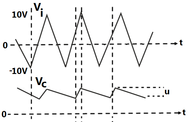
Sign in to UnlockThe figure shows a half-wave rectifier with a 475 filter capacitor. The load draws a constant current from the rectifier. The figure also shows the input voltage , the output voltage and the peak-to-peak voltage ripple u on. The input voltage is a triangle-wave with amplitude of 10 V and a period of 1ms.


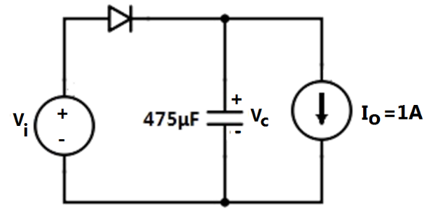
The value of the ripple u (in volts) is __________.
Sign in to see the solution
Log in to view the explanation, track your attempts, and keep your progress.
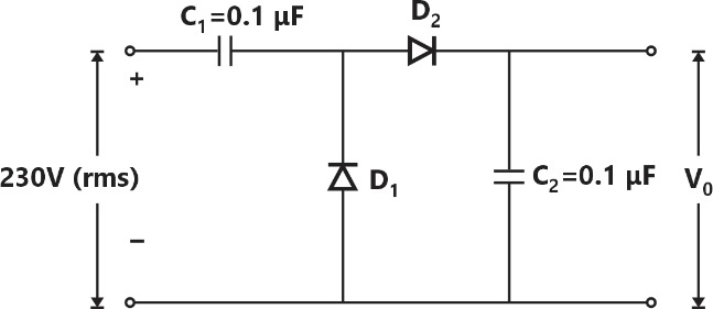
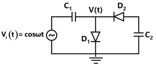
Sign in to UnlockThe diodes and in the figure are ideal and the capacitors are identical. The product RC is very large compared to the time period of the ac voltage. Assuming that the diodes do not breakdown in the reverse bias, the output voltage (in volt) at the steady state is _________.


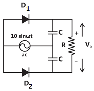
Sign in to see the solution
Log in to view the explanation, track your attempts, and keep your progress.
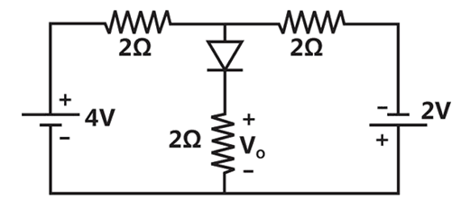
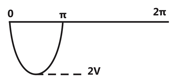
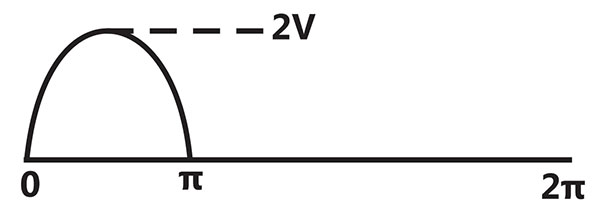
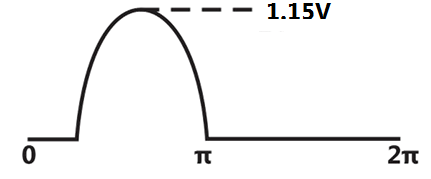
Sign in to UnlockFor the circuit with ideal diodes shown in the figure, the shape of the output () for the given sine wave input () will be

Sign in to see the solution
Log in to view the explanation, track your attempts, and keep your progress.
Sign in to UnlockIn the circuit shown below, the Zener diode is ideal and the Zener voltage is 6V. The output voltage (in volts) is _______.

Sign in to see the solution
Log in to view the explanation, track your attempts, and keep your progress.
Sign in to UnlockIf the circuit shown has to function as a clamping circuit, then which one of the following conditions should be satisfied for the sinusoidal signal of period T?
Sign in to see the solution
Log in to view the explanation, track your attempts, and keep your progress.
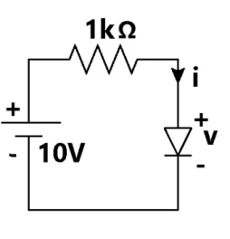
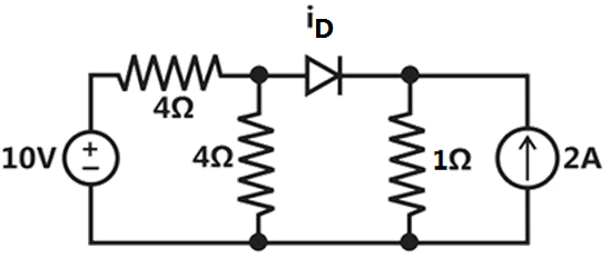
Sign in to UnlockThe diode in the circuit given below has but is ideal otherwise. The current (in mA) in the 4 kΩ resistor is _______.

Sign in to see the solution
Log in to view the explanation, track your attempts, and keep your progress.
Sign in to UnlockIn the circuit shown, assume that diodes and are ideal. In the steady state condition, the average voltage (in Volts) across the 0.5μF capacitor is _____.

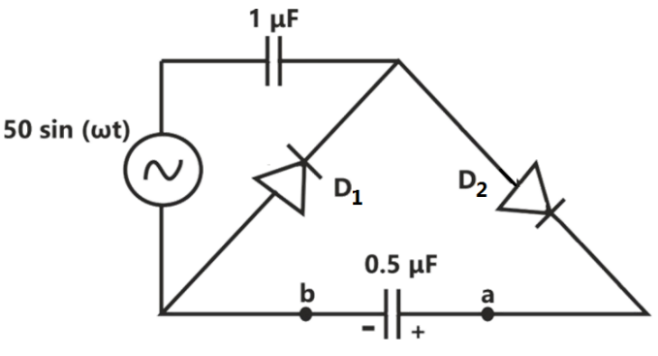
Sign in to see the solution
Log in to view the explanation, track your attempts, and keep your progress.
Sign in to UnlockIn the circuit shown, assume that the diodes and are ideal. The average value of voltage (in Volts), across terminals ‘a’ and ‘b’ is _________.
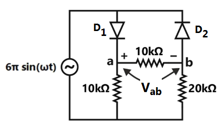
Sign in to see the solution
Log in to view the explanation, track your attempts, and keep your progress.
Sign in to UnlockIn the figure assume that the forward voltage drops of the PN diode and Schottky Diode are 0.7V and 0.3v respectively. If ON denotes conduction state of the diode and OFF denoted non-conduction sate of the diode, then the circuit,
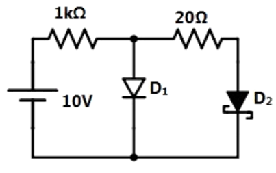
both and are ON
is ON and is OFF
Both and are OFF
is OFF and is ON
Sign in to see the solution
Log in to view the explanation, track your attempts, and keep your progress.
Sign in to UnlockThe diode in the circuit shown has Volts but is ideal otherwise. If Volts, the minimum and maximum values of (in Volts) are, respectively,


Sign in to see the solution
Log in to view the explanation, track your attempts, and keep your progress.
Sign in to UnlockThe figure shows a half-wave rectifier. The diode D is ideal. The average steady-state current (in Amperes) through the diode is approximately ____________.
Sign in to see the solution
Log in to view the explanation, track your attempts, and keep your progress.
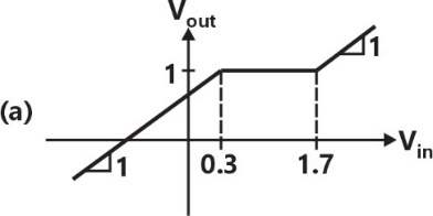
Sign in to UnlockTwo silicon diodes, with a forward voltage drop of 0.7 V, are used in the circuit shown in the figure. The range of input voltage for which the output voltage, is


Sign in to see the solution
Log in to view the explanation, track your attempts, and keep your progress.
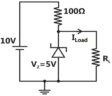
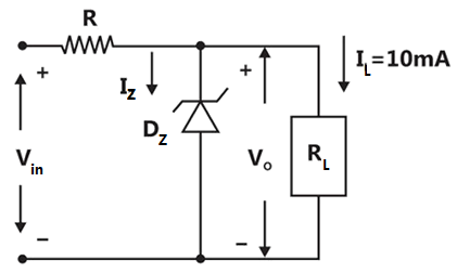
Sign in to UnlockIn the circuit shown below, the knee current of the ideal Zener diode is 10mA. To maintain 5 V across , the minimum value of in and the minimum power rating of the Zener diode in mW, respectively, are


Sign in to see the solution
Log in to view the explanation, track your attempts, and keep your progress.
Sign in to UnlockA voltage Volts is applied across YZ. Assuming ideal diodes, the voltage measured across WX in Volts, is

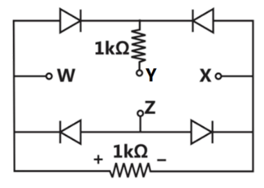


0 for all t
Sign in to see the solution
Log in to view the explanation, track your attempts, and keep your progress.
Sign in to UnlockThe I-V characteristics of the diode in the circuit given below are

The current in the circuit is
Sign in to see the solution
Log in to view the explanation, track your attempts, and keep your progress.
Sign in to UnlockThe diodes and capacitors in the circuit shown are ideal. The voltage v(t) across the diode D1 is
Sign in to see the solution
Log in to view the explanation, track your attempts, and keep your progress.
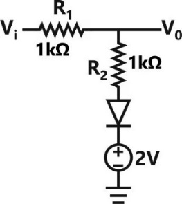
Sign in to UnlockIn the circuit shown below, assume that the voltage drop across a forward biased diode is 0.7 V. The thermal voltage . The small signal input where .


The bias current through the diodes is

Sign in to see the solution
Log in to view the explanation, track your attempts, and keep your progress.
Sign in to UnlockIn the circuit shown below, assume that the voltage drop across a forward biased diode is 0.7 V. The thermal voltage . The small signal input where .
The ac output voltage is


Sign in to see the solution
Log in to view the explanation, track your attempts, and keep your progress.
Sign in to UnlockIn the circuit below, the diode is ideal. The voltage V is given by
min (, 1)

max (, 1)
min (, 1)

max (, 1)
Sign in to see the solution
Log in to view the explanation, track your attempts, and keep your progress.
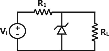
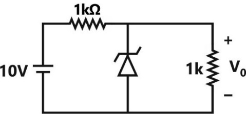
Sign in to UnlockIn the following limiter circuit, an input voltage is applied. Assume that the diode drop is when it is forward biased. The Zener breakdown voltage is . The maximum and minimum values of the output voltage respectively are


Sign in to see the solution
Log in to view the explanation, track your attempts, and keep your progress.
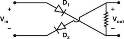
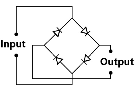
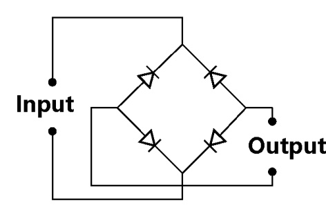
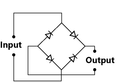
Sign in to UnlockThe correct full-wave rectifier circuit is
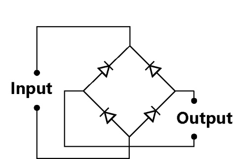
Sign in to see the solution
Log in to view the explanation, track your attempts, and keep your progress.
Sign in to UnlockFor the Zener diode shown in the figure, the Zener voltage at knee is 7 V, the knee current is negligible and the Zener dynamic resistance is 10 Ω. If the input voltage range is from 10 to 16V, the output voltage ranges from


Sign in to see the solution
Log in to view the explanation, track your attempts, and keep your progress.
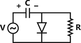
Sign in to UnlockFor the circuit shown below, assume that the zener diode is ideal with a breakdown voltage of 6 Volts. The waveform observed across R is:
Sign in to see the solution
Log in to view the explanation, track your attempts, and keep your progress.
Sign in to UnlockThe Zener diode in the regulator circuit shown in figure has a Zener voltage of 5.8 Volts and a Zener knee current of 0.5mA. The maximum load current drawn from this circuit ensuring proper functioning over the input voltage range between 20 and 30 Volts, is
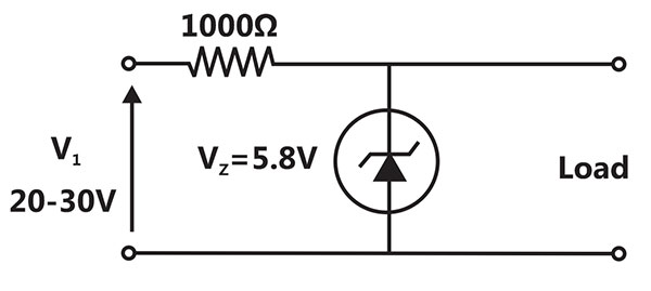
Sign in to see the solution
Log in to view the explanation, track your attempts, and keep your progress.
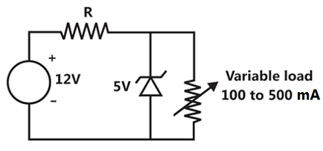
Sign in to UnlockIn the voltage regulator shown in Figure, the load current can vary from 100mA to 500mA. Assuming that the Zener diode is ideal (i.e., the Zener knee current is negligibly small and Zener resistance is zero in the breakdown region), the value of R is


Sign in to see the solution
Log in to view the explanation, track your attempts, and keep your progress.
Sign in to UnlockIn a full-wave rectifier using two ideal diodes, and are the dc and peak values of the voltage respectively across a resistive load. If PIV is the peak inverse voltage of the diode, then the appropriate relationships for this rectifier are


,


,

,

,
Sign in to see the solution
Log in to view the explanation, track your attempts, and keep your progress.
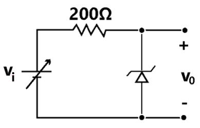
Sign in to UnlockThe circuit shown in the figure is best described as a
Sign in to see the solution
Log in to view the explanation, track your attempts, and keep your progress.
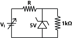
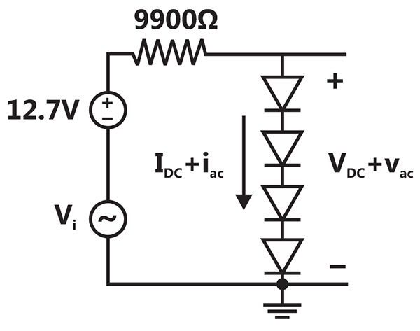
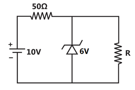
Sign in to UnlockA zener diode regulator in Figure is to be designed to meet the specifications:
, and varies from 30 V to 50 V. The zener diode has and (knee current) = 1 mA. For satisfactory operation


Sign in to see the solution
Log in to view the explanation, track your attempts, and keep your progress.
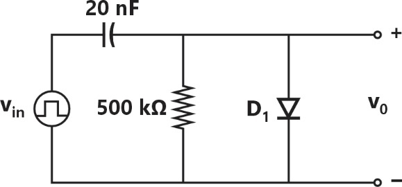
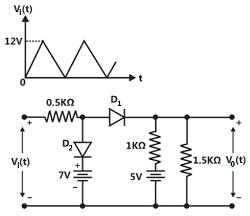
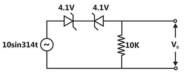
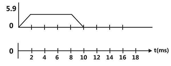
Sign in to UnlockA triangular voltage waveform is applied at the input to the circuit of figure shown below. Assume the diodes to be ideal.

(a) Determine the output .

(b) Neatly sketch the output waveform superimposed on the input and label the key points.

Sign in to see the solution
Log in to view the explanation, track your attempts, and keep your progress.
Sign in to UnlockFor the circuit shown in Figure, and are identical diodes with ideality factor of unity. The thermal voltage

(a) Calculate and


(b) If the reverse saturation current, for the diode is 1pA, then compute the current I through the circuit.

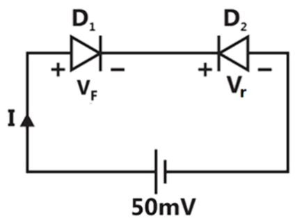
(a)

(a)
(b) I = 0.99pA
(b) I = 1.99pA
Sign in to see the solution
Log in to view the explanation, track your attempts, and keep your progress.
Sign in to UnlockFor the circuit in Figure, the voltage is

Sign in to see the solution
Log in to view the explanation, track your attempts, and keep your progress.
Sign in to Unlock(a) For figure, Plot under steady state conditions, with and without C. Assume that the diode is ideal.

(b) Design a circuit using two ideal diodes, one resistor and two voltage sources that would convert the input voltage to the output voltage which is shown below. The resistor value need not be specified.
(a) With capacitor
(a) Without capacitor
(b)
(b)
Sign in to see the solution
Log in to view the explanation, track your attempts, and keep your progress.
Sign in to UnlockA dc power supply has a no-load voltage of 30V and a full-load voltage of 25 V at a full-load current of 1A. Its output resistance and load regulation respectively are
and 20%

and 20%

and 16.7%
and 16.7%
Sign in to see the solution
Log in to view the explanation, track your attempts, and keep your progress.
Sign in to UnlockFor full wave rectification, a four diode bridge rectifier is claimed to have the following advantages over a two diode circuit:
(1) Less expensive transformer
(2) Smaller size transformer, and
(3) Suitability for higher voltage application.
Of these,
Sign in to see the solution
Log in to view the explanation, track your attempts, and keep your progress.
Sign in to UnlockFor a small signal AC operation, a practical forward biased diode can be modelled as
Sign in to see the solution
Log in to view the explanation, track your attempts, and keep your progress.
Sign in to UnlockFor a given circuit
(a) Draw the transfer characteristic of the circuit of Figure, assuming both and to be ideal.


(b) How would the characteristic change if is ideal, but is non-ideal in that it has forward resistance of and a reverse resistance of infinity?

(a) Transfer characteristic
(b) Transfer characteristic
(a) This circuit doesn’t exist.
(b) Transfer characteristic
Sign in to see the solution
Log in to view the explanation, track your attempts, and keep your progress.
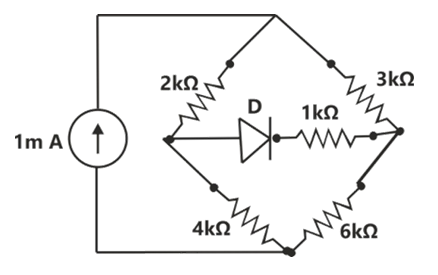
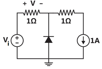
Sign in to UnlockIn the circuit of the figure is the current through the ideal diode (zero cut in voltage and forward resistance) equals

Sign in to see the solution
Log in to view the explanation, track your attempts, and keep your progress.
Sign in to UnlockA half wave rectifier uses a diode with a forward resistance The voltage is sin and the load resistance is . The DC current is given by


Sign in to see the solution
Log in to view the explanation, track your attempts, and keep your progress.
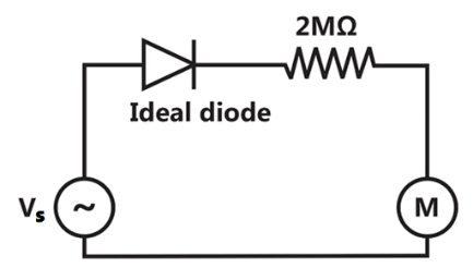
Sign in to UnlockIn the circuit of the given figure, assume that the diodes are ideal and the meter is an average indicating ammeter. The ammeter will read

0.4 mA

mA

Sign in to see the solution
Log in to view the explanation, track your attempts, and keep your progress.
Sign in to UnlockA zener diode in the circuit shown in the figure has a knee current of 5mA, and a maximum allowed power dissipation of 300mW. What are the minimum and maximum load currents that can be drawn safety from the circuit, keeping the output voltage constant at 6V?

Sign in to see the solution
Log in to view the explanation, track your attempts, and keep your progress.
Sign in to UnlockThe forward dynamic resistance of a junction diode varies inversely as the forward current ( True=1, False=0)
Sign in to see the solution
Log in to view the explanation, track your attempts, and keep your progress.
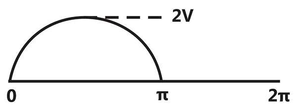
Sign in to UnlockThe wave shape of in figure will be

Sign in to see the solution
Log in to view the explanation, track your attempts, and keep your progress.
Sign in to UnlockIn the figure, is in ideal moving iron voltmeter M will read
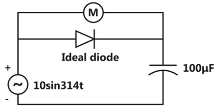
Sign in to see the solution
Log in to view the explanation, track your attempts, and keep your progress.
Sign in to UnlockM in figure is a rectifier type 200V full scale voltmeter having a sensitivity of 10kΩ/Volt what will be the reading in M if the source voltage is a symmetrical square wave of 800 volts peal to peak?

Sign in to see the solution
Log in to view the explanation, track your attempts, and keep your progress.
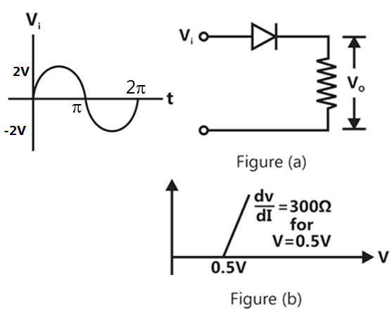
Sign in to UnlockConsider the circuit shown in figure (a). If the diode used here has the V-I characteristic as in figure (b), then the output wave form is:

Sign in to see the solution
Log in to view the explanation, track your attempts, and keep your progress.
Sign in to UnlockThe 6V zener diode shown in figure has zero zener resistance and a knee current of 5mA. The minimum value of R so that the voltage across it does not fall below 6V is
Sign in to see the solution
Log in to view the explanation, track your attempts, and keep your progress.
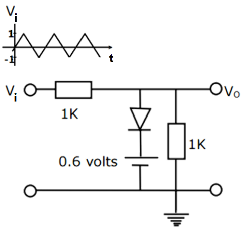
Sign in to UnlockIn figure the input is a 100 Hz triangular wave having a peak to peak amplitude of 2 volts and an average value of zero volts. Given that the diode is ideal, the average value of the output is __________.
Sign in to see the solution
Log in to view the explanation, track your attempts, and keep your progress.
Sign in to Unlock