Digital Electronics
Memory
Practice questions from Memory.
19
Total0
Attempted0
Correct0
IncorrectA ROM array is built with the help of diodes as shown in the circuit below. Here WO and W1 are signals that select the word lines and BO and B1 are signals that are output of the sense amps based on the stored data corresponding to the bit lines during the read operation.


Bits stored in the ROM Array
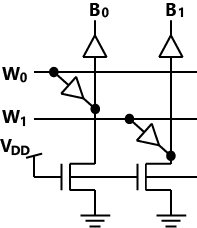
During the read operation, the selected word line goes high and the other word line is in a high impedance state. As per the implementation shown in the circuit diagram above, what are the bits corresponding to (where = 0 or 1 and j = 0 or 1) stored in the ROM?


Sign in to see the solution
Log in to view the explanation, track your attempts, and keep your progress.
Sign in to UnlockIn a DRAM,
Sign in to see the solution
Log in to view the explanation, track your attempts, and keep your progress.
Sign in to UnlockAn 8 Kbyte ROM with an active low Chip Select input is to be used in an 8085 microprocessor based system. The ROM should occupy the address range 1000H to 2FFFH. The address lines are designated as to , where is the most significant address bit. Which one of the following logic expressions will generate the correct signal for this ROM?


Sign in to see the solution
Log in to view the explanation, track your attempts, and keep your progress.
Sign in to UnlockA 16 Kb (=16,384 bit) memory array is designed as a square with an aspect ratio of one (number of rows is equal to the number of columns). The minimum number of address lines needed for the row decoder is _______.
Sign in to see the solution
Log in to view the explanation, track your attempts, and keep your progress.
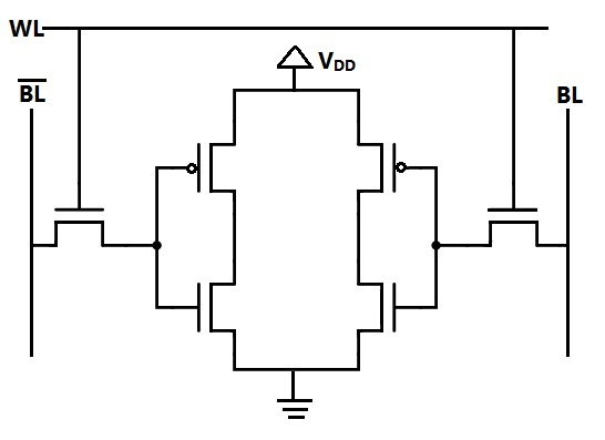
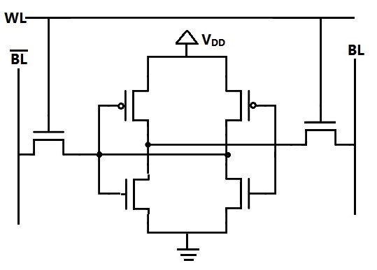
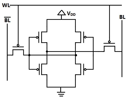
Sign in to UnlockIf WL is the Word Line and BL the Bit Line, an SRAM cell is shown in
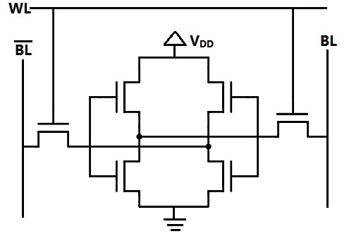
Sign in to see the solution
Log in to view the explanation, track your attempts, and keep your progress.
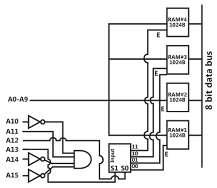
Sign in to UnlockThere are four chips each of 1024 bytes connected to a 16 bit address bus as shown in the figure below. RAMs 1, 2, 3 and 4 respectively are mapped to addresses
Sign in to see the solution
Log in to view the explanation, track your attempts, and keep your progress.
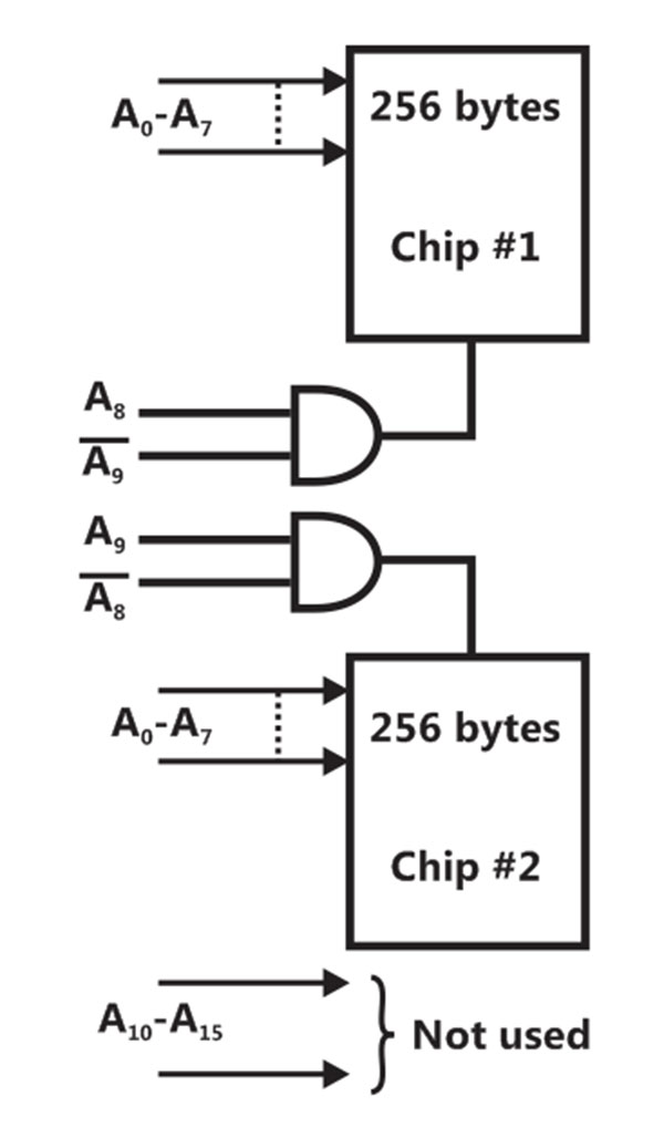
Sign in to UnlockWhat memory address range is NOT represented by chip #1 and chip #2 in figure? to in this figure are the address lines and CS means Chip Select.
Sign in to see the solution
Log in to view the explanation, track your attempts, and keep your progress.
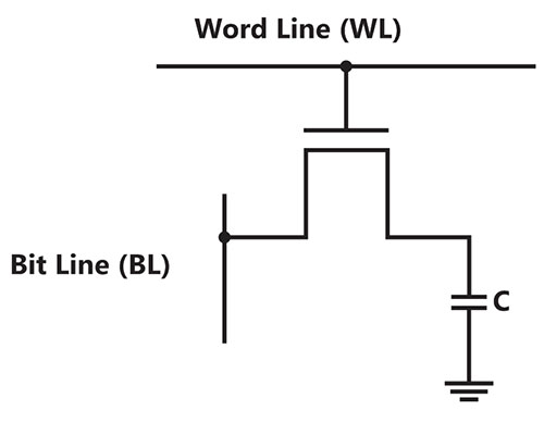
Sign in to UnlockIn the DRAM cell in Figure, the of the NMOSFET is 1 V. For the following three combinations of WL, C and BL voltages

Sign in to see the solution
Log in to view the explanation, track your attempts, and keep your progress.
Sign in to UnlockEach cell of a static Random Access Memory contains
Sign in to see the solution
Log in to view the explanation, track your attempts, and keep your progress.
Sign in to UnlockThe gate delay of a NMOS inverter is dominated by charge time rather than discharge time because
Sign in to see the solution
Log in to view the explanation, track your attempts, and keep your progress.
Sign in to UnlockMatch the following
(1) An 8-bit wide 4-word sequential memory will have
(2) A EPROM has

(a) 8 fixed ‘AND’ gates and 4 Programmable ‘OR’ gates
(b) Eight 4 bit shift registers
(c) 4 words of 32 bits each
(d) 8 address pins and 4 data pins output
Sign in to see the solution
Log in to view the explanation, track your attempts, and keep your progress.
Sign in to UnlockA dynamic RAM cell which hold 5 V has to be refreshed every 20 m secs, so that the stored voltage does not fall by more than 0.5V. If the cell has a constant discharge current of 0.1pA, the storage capacitance of the cell is


Sign in to see the solution
Log in to view the explanation, track your attempts, and keep your progress.
Sign in to UnlockA memory system of size 26 K bytes is required to be designed using memory chips which have 12 address lines and 4 data lines each. The number of such chips required to design the memory system is
Sign in to see the solution
Log in to view the explanation, track your attempts, and keep your progress.
Sign in to UnlockThe minimum number of MOS transistors required to make a dynamic RAM cell is
Sign in to see the solution
Log in to view the explanation, track your attempts, and keep your progress.
Sign in to UnlockA PLA can be used
Sign in to see the solution
Log in to view the explanation, track your attempts, and keep your progress.
Sign in to UnlockA dynamic RAM consists of
Sign in to see the solution
Log in to view the explanation, track your attempts, and keep your progress.
Sign in to UnlockChoose the correct statement(s) from the following:
Sign in to see the solution
Log in to view the explanation, track your attempts, and keep your progress.
Sign in to UnlockTwo dimensional addressing of bit ROM using to 8:1 selectors requires ________ (how many?) NAND gates

Sign in to see the solution
Log in to view the explanation, track your attempts, and keep your progress.
Sign in to UnlockA bit stored in a FAMOS device can be erased by UV Light. (True=1, False=0)
Sign in to see the solution
Log in to view the explanation, track your attempts, and keep your progress.
Sign in to Unlock