Digital Electronics
Microprocessor
Practice questions from Microprocessor.
57
Total0
Attempted0
Correct0
IncorrectThe content of the registers are , and . The following machine instructions are executed,


PUSH

PUSH

PUSH


After execution, the content of registers are


Sign in to see the solution
Log in to view the explanation, track your attempts, and keep your progress.
Sign in to UnlockIn an 8085 microprocessor, the number of address lines required to access a  byte memory bank is _______.
Sign in to see the solution
Log in to view the explanation, track your attempts, and keep your progress.
Sign in to UnlockThe clock frequency of an 8085 microprocessor is 5 MHz. If the time required to execute an instruction is 1.4 µs, then the number of T-states needed for executing the instruction is
Sign in to see the solution
Log in to view the explanation, track your attempts, and keep your progress.
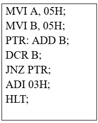
Sign in to UnlockThe following FIVE instructions were executed on an 8085 microprocessor.
MVI A, 33H
MVI B, 78H
ADD B
CMA
ANI 32 H
The Accumulator value immediately after the execution of the fifth instruction is
Sign in to see the solution
Log in to view the explanation, track your attempts, and keep your progress.
Sign in to UnlockIn an 8085 system, a PUSH operation requires more clock cycles than a POP operation.
Which one of the following options is the correct reason for this?
Sign in to see the solution
Log in to view the explanation, track your attempts, and keep your progress.
Sign in to UnlockIn an 8085 microprocessor, the contents of the accumulator and the carry flag are A7 (in hex) and 0, respectively. If the instruction RLC is executed, then the contents of the accumulator (in hex) and the carry flag respectively, will be
Sign in to see the solution
Log in to view the explanation, track your attempts, and keep your progress.
Sign in to UnlockIn an 8085 microprocessor, the shift registers which store the result of an addition and the overflow bit are, respectively
Sign in to see the solution
Log in to view the explanation, track your attempts, and keep your progress.
Sign in to UnlockIn an 8085 microprocessor, which one of the following instructions changes the content of the accumulator?
Sign in to see the solution
Log in to view the explanation, track your attempts, and keep your progress.
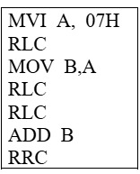
Sign in to UnlockWhich one of the following 8085 microprocessor programs correctly calculates the product of two 8-bit numbers stored in registers B and C?
Sign in to see the solution
Log in to view the explanation, track your attempts, and keep your progress.
Sign in to UnlockFor the 8085 microprocessor, the interfacing circuit to input 8-bit digital data from an external device is shown in the figure. The instruction for correct data transfer is

Sign in to see the solution
Log in to view the explanation, track your attempts, and keep your progress.
Sign in to UnlockAn 8085 microprocessor executes “STA 1234H” with starting address location 1FFEH (STA copies the contents of the Accumulator to the 16-bit address location). While the instruction is fetched and executed, the sequence of values written at the address pins is

Sign in to see the solution
Log in to view the explanation, track your attempts, and keep your progress.
Sign in to UnlockFor 8085 microprocessor, the following program is executed.
At the end of program, accumulator contains
Sign in to see the solution
Log in to view the explanation, track your attempts, and keep your progress.
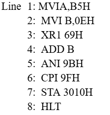
Sign in to UnlockAn 8085 assembly language program is given below. Assume that the carry flag is initially unset. The content of the accumulator after the execution of the program is
Sign in to see the solution
Log in to view the explanation, track your attempts, and keep your progress.
Sign in to UnlockFor the 8085 assembly language program given below, the content of the accumulator after the execution of the program is
Sign in to see the solution
Log in to view the explanation, track your attempts, and keep your progress.
Sign in to UnlockIn microprocessor, the service routine for a certain interrupt starts from a fixed location of memory which cannot be externally set, but the interrupt can be delayed or rejected. Such an interrupt is
Sign in to see the solution
Log in to view the explanation, track your attempts, and keep your progress.
Sign in to UnlockAn 8085 assembly language program is given below.
After execution of line 7 of the program, the status of the CY and Z flags will be
Sign in to see the solution
Log in to view the explanation, track your attempts, and keep your progress.
Sign in to UnlockAn 8085 executes the following instructions
2710 LXI H, 30A0H
2713 DAD H
2714 PCHL
All addresses and constants are in Hex. Let PC be the contents of the program counter and HL be the contents of the HL register pair just after executing PCHL.
Which of the following statements is correct?
Sign in to see the solution
Log in to view the explanation, track your attempts, and keep your progress.
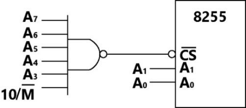
Sign in to UnlockAn 8255 chip is interfaced to an 8085 microprocessor system as an I/O mapped I/O as shown in the figure. The address lines and of the 8085 are used by the 8255 chip to decode internally its three ports and the Control register. The address lines. to as well as signal are used for address decoding. The range of addresses for which the 8255 chip would get selected is


Sign in to see the solution
Log in to view the explanation, track your attempts, and keep your progress.
Sign in to UnlockAn 8085 assembly language program is given below.
he contents of the accumulator just after execution of the ADD instruction inline 4 will be
Sign in to see the solution
Log in to view the explanation, track your attempts, and keep your progress.
Sign in to UnlockFollowing is the segment of a 8085 assembly language program:
LXI SP, EFFF H
CALL 3000 H
:
:
3000 H: LXI H, 3CF4 H
PUSH PSW
SPHL
POP PSW
RET
On completion of RET execution, the contents of SP is
Sign in to see the solution
Log in to view the explanation, track your attempts, and keep your progress.
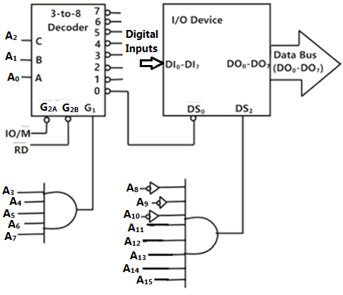
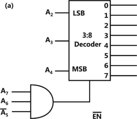
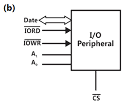
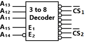
Sign in to UnlockAn I/O peripheral device shown in figure (b) below is to be interfaced to an 8085 microprocessor. To select the I/O device in the I/O address range D4 H – D7 H, its chip-select should be connected to the output of the decoder shown in figure (a) below

Sign in to see the solution
Log in to view the explanation, track your attempts, and keep your progress.
Sign in to UnlockConsider an 8085-microprocessor system.
The following program starts at location 0100H.
The content of accumulator when the program counter reaches 0109H is
Sign in to see the solution
Log in to view the explanation, track your attempts, and keep your progress.
Sign in to UnlockConsider an 8085-microprocessor system.
The following program starts at location 0100H.
If in addition following code exists from 0109H onwards.
ORI 40H
ADD M
What will be the result in the accumulator after the last instruction is executed?
Sign in to see the solution
Log in to view the explanation, track your attempts, and keep your progress.
Sign in to UnlockThe 8255 Programmable Peripheral Interface is used as described below.
I. An A/D converter is interfaced to a microprocessor through an 8255. The conversion is initiated by a signal from the 8255 on port C. A signal on port C causes data to be stored into port A.
II. Two computers exchange data using a pair of 8255s. Port A works as a bi-directional data port supported by appropriate handshaking signals.
The appropriate modes of operation of the 8255 for I and II would be
Sign in to see the solution
Log in to view the explanation, track your attempts, and keep your progress.
Sign in to UnlockThe number of memory cycles required to execute the following 8085 instructions
I. LDA 3000H
II. LXI D, FOF 1H
Would be
Sign in to see the solution
Log in to view the explanation, track your attempts, and keep your progress.
Sign in to UnlockConsider the sequence of 8085 instructions given below.
LXI H, 9258
MOV A,M
CMA
MOV M,A
Which one of the following is performed by this sequence?
Sign in to see the solution
Log in to view the explanation, track your attempts, and keep your progress.
Sign in to UnlockIt is desired to multiply the numbers 0AH by 0BH and store the result in the accumulator. The numbers are available in registers B and C respectively. A part of the 8085 program for this purpose is given below:
The sequence of instruction to the complete the program would be
Sign in to see the solution
Log in to view the explanation, track your attempts, and keep your progress.
Sign in to UnlockIn an 8085 microprocessor, the instruction CMP B has been executed while the content of the accumulator is less than that of register B. As a result
Sign in to see the solution
Log in to view the explanation, track your attempts, and keep your progress.
Sign in to UnlockConsider the following assembly language program.
The execution of the above program in an 8085 microprocessor will result in
Sign in to see the solution
Log in to view the explanation, track your attempts, and keep your progress.
Sign in to UnlockAn 8085 microprocessor operating at 5 MHz clock frequency execute the following routine.
(a) Determine the total number of machine cycles required to execute this routine till the JMP instruction is executed for the first time.
(b) Determine the time interval between two consecutive signals.

(c) If the external logic controls the READY line so that three WAIT states are introduced in the I/O WRITE machine cycle, determine the time interval between two consecutive signals.
Sign in to see the solution
Log in to view the explanation, track your attempts, and keep your progress.
Sign in to UnlockAn 8085 microprocessor based system uses a 4K × 8-bit RAM whose starting address is AA00. The address of the last byte in this RAM is
Sign in to see the solution
Log in to view the explanation, track your attempts, and keep your progress.
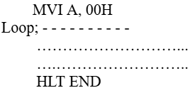
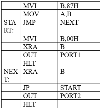
Sign in to UnlockConsider the following sequence of instructions for an 8085 microprocessor-based system:
(a) If the program execution begins at the location FF00 H, write down the sequence of instructions which are actually executed till a HLT instruction. (Assume all flags are initially RESET)
(b) Which of three ports (PORT1, PORT2 and PORT3) will be loaded with the data and what is the bit pattern of the data?
(a) The actual sequence of instructions being executed is,
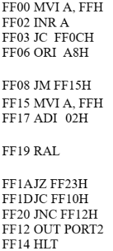
(b) PORT 2 is loaded with output data and the bit pattern is 0000 0011
(b) PORT 3 is loaded with output data and the bit pattern is 0000 0011
None
Sign in to see the solution
Log in to view the explanation, track your attempts, and keep your progress.
Sign in to UnlockThe contents of Register (B) and Accumulator (A) of 8085 microprocessor are 49H and 3AH respectively. The contents of A and the status of carry flag (CY) and sign flag (S) after executing SUB B instructions are
Sign in to see the solution
Log in to view the explanation, track your attempts, and keep your progress.
Sign in to UnlockThe number of hardware interrupts (which require an external signal to interrupt) present in an 8085 microprocessor are
Sign in to see the solution
Log in to view the explanation, track your attempts, and keep your progress.
Sign in to UnlockIn the 8085 microprocessor, the RST6 instruction transfers the program execution to the following location
Sign in to see the solution
Log in to view the explanation, track your attempts, and keep your progress.
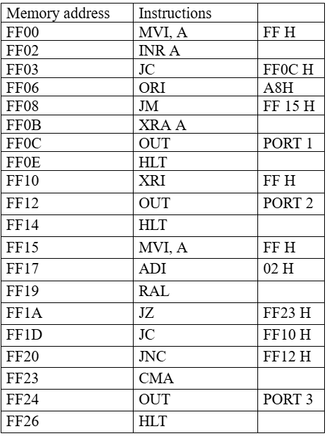
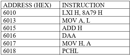
Sign in to Unlock(a) The program and machine code for an 8085 microprocessor are given by
The starting address of the above program is 7FFF H. What would happen if it is executed from 8000 H?
(b) For the instructions given below, how many memory operations (read/write) are performed during the execution in an ?

(c) Write an instruction which takes the minimum possible time to clear the accumulator of the 8085.
Sign in to see the solution
Log in to view the explanation, track your attempts, and keep your progress.
Sign in to UnlockIf is used as the chip select logic of a 4 KRAM in an 8085 system, then its memory range will be

Sign in to see the solution
Log in to view the explanation, track your attempts, and keep your progress.
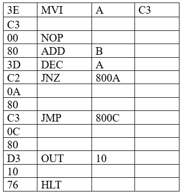
Sign in to UnlockAn 8085 assembly language program is given below:
Contents of the memory locations 2000 H to 2002H are:
2000 : 18 H 2001 : 10H 2002 : 2BH
(a) What does the above program do?
(b) At the end of the program, what will be
(i) The contents of the registers A, B, C ,H and L?
(ii) The condition of the carry and zero flags?
(iii) The contents of the memory locations 2000 H, 2001 H , 2002 H and 2100 H.
Sign in to see the solution
Log in to view the explanation, track your attempts, and keep your progress.
Sign in to UnlockAn I/O processor control the flow of information between
Sign in to see the solution
Log in to view the explanation, track your attempts, and keep your progress.
Sign in to UnlockWrite a short assembly language program, without using any arithmetic instruction, to store hexadecimal 5D in the flag register of 8085 microprocessor. Data in other registers of the processor must not alter upon executing this program.
Sign in to see the solution
Log in to view the explanation, track your attempts, and keep your progress.
Sign in to UnlockAn instruction used to set the carry Flag in a computer can be classified as
Sign in to see the solution
Log in to view the explanation, track your attempts, and keep your progress.
Sign in to UnlockIn an system, the RST instruction will cause an interrupt
Sign in to see the solution
Log in to view the explanation, track your attempts, and keep your progress.
Sign in to UnlockThe following instructions have been executed by an 8085 .

From which address will the next instruction be fetched?
Sign in to see the solution
Log in to view the explanation, track your attempts, and keep your progress.
Sign in to UnlockA signed integer has been stored in a byte using the 2’s complement format. We wish to store the same integer in a 16 bit word. We should
Sign in to see the solution
Log in to view the explanation, track your attempts, and keep your progress.
Sign in to UnlockWhile moving data between registers of the 8085 and the stack
(1) A PUSH instruction
(2) A POP instruction
Sign in to see the solution
Log in to view the explanation, track your attempts, and keep your progress.
Sign in to UnlockAn uses a 2 MHz crystal. Find the time taken by it to execute the following delay subroutine, inclusive of the call instruction in the calling program.
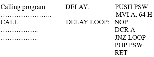
You are given that a CALL instruction takes 18 cycles of the system clock, PUSH requires 12 cycles and a conditional jump takes 10 cycles if the jump is taken and 7 cycles if it is not. All other instructions used
above take clock cycles, where n is the number of accesses to the memory, inclusive of the op-code fetch.

Sign in to see the solution
Log in to view the explanation, track your attempts, and keep your progress.
Sign in to UnlockThe total number of memory accesses involved (inclusive of the op-code fetch) when an 8085 processor executes the instruction LDA 2003 is
Sign in to see the solution
Log in to view the explanation, track your attempts, and keep your progress.
Sign in to UnlockWhen CPU is interrupted, it
Sign in to see the solution
Log in to view the explanation, track your attempts, and keep your progress.
Sign in to UnlockA ‘DMA’ transfer implies
Direct transfer of data between memory and accumulator
Direct transfer of data between memory and I/O devices without the use of

Transfer of data exclusively within registers
A fast transfer of data between and I/O devices
Sign in to see the solution
Log in to view the explanation, track your attempts, and keep your progress.
Sign in to UnlockAn ‘Assembler’ for a microprocessor is used for
Sign in to see the solution
Log in to view the explanation, track your attempts, and keep your progress.
Sign in to UnlockIn a microprocessor, the register which holds the address of the next instruction to be fetched is:
Sign in to see the solution
Log in to view the explanation, track your attempts, and keep your progress.
Sign in to UnlockIn a microcomputer, wait states are used at
Sign in to see the solution
Log in to view the explanation, track your attempts, and keep your progress.
Sign in to UnlockA microprocessor has five address lines and eight data lines . An input device A, an output device B, A ROM and a RAM are memory mapped to the microprocessor at the addresses as shown in figure.


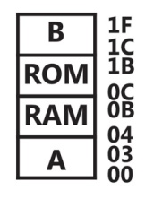
Devices A and B have four addressable registers each; RAM has 8 bytes and ROM has 16 bytes.
Obtain the minimum sum of product expression for the chip select (CS) function of each device/memory.


Sign in to see the solution
Log in to view the explanation, track your attempts, and keep your progress.
Sign in to UnlockIn an 8085 microprocessor system with memory mapped I/O,
Sign in to see the solution
Log in to view the explanation, track your attempts, and keep your progress.
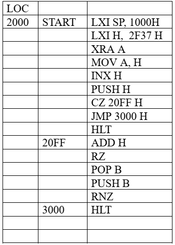
Sign in to UnlockThe following program is run on 8085 microprocessor:
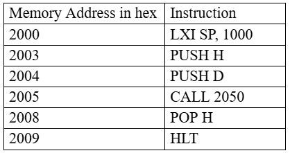
At the completion of execution of the program, the program Counter of the 8085 contains __________ and the Stack Pointer contains __________.


Sign in to see the solution
Log in to view the explanation, track your attempts, and keep your progress.
Sign in to UnlockFigure shows the memory circuit of an 8085 microprocessor.
(a) What is the total size of the memory in the circuit?
(b) What are the beginning and ending addresses of the memory in chip 1?
(Give the answer in hexadecimal numbers)
(c) What are the beginning and ending addresses of the memory in chip 2?
(d) Are the memory chips in the circuit ROM or RAM?
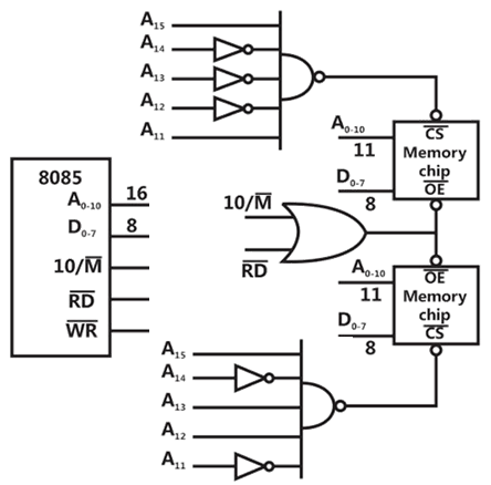
(e) How will you replace the two NAND gates in the circuit with one 3 to 8 decoder without changing the memory addresses? Assume that the decoder has one active high enable and one active low enable .


Total size of memory
The chips used in the circuit are ROM

Beginning and ending addresses of the memory in chip 1

Beginning and ending addresses of the memory in chip 2

Sign in to see the solution
Log in to view the explanation, track your attempts, and keep your progress.
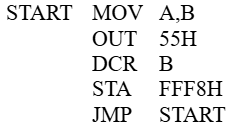
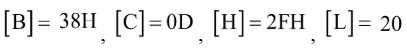
Sign in to UnlockThe program given below is run on an 8085 based microcomputer system. Determine the contents of the registers: PC, SP, B, C, H, L after a halt instruction is executed.

, , ,


Sign in to see the solution
Log in to view the explanation, track your attempts, and keep your progress.
Sign in to Unlock