Digital Electronics
Combinational Circuits
Practice questions from Combinational Circuits.
48
Total0
Attempted0
Correct0
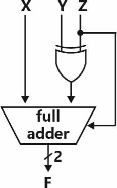
IncorrectA full adder and an XOR gate are used to design a digital circuit with inputs , and , and output , as shown below. The input is connected to the carry-in input of the full adder.


If the input is set to logic ' ', then the circuit functions as _________ with and as inputs.


Sign in to see the solution
Log in to view the explanation, track your attempts, and keep your progress.
Sign in to UnlockA 4-bit priority encoder has inputs , and in descending order of priority. The two-bit output is generated as , and 11 corresponding to inputs , and , respectively. The Boolean expression of the output bit is_____.


Sign in to see the solution
Log in to view the explanation, track your attempts, and keep your progress.
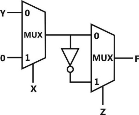
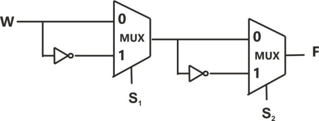
Sign in to UnlockThe propagation delay of the MUX shown in the circuit is 10 ns. Consider the propagation delay of the inverter as .


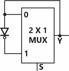
If is set to 1 then the output is________.


a square wave of frequency

a square wave of frequency

constant at 0
constant at 1
Sign in to see the solution
Log in to view the explanation, track your attempts, and keep your progress.
Sign in to UnlockIn the circuit shown below, and are the inputs. The logical function realized by the circuit shown below is


Sign in to see the solution
Log in to view the explanation, track your attempts, and keep your progress.
Sign in to UnlockFor the circuit shown below, the propagation delay of each NAND gate is . The critical path delay, in ns, is ________ (rounded off to the nearest integer).

Sign in to see the solution
Log in to view the explanation, track your attempts, and keep your progress.
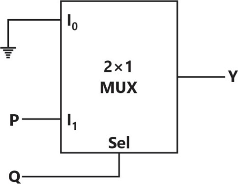
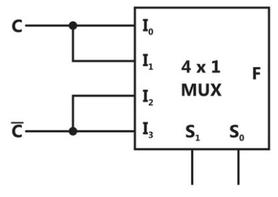
Sign in to UnlockConsider the 2-bit multiplexer (MUX) shown in the figure. For OUTPUT to be the XOR of and , the values for and are ________.


Sign in to see the solution
Log in to view the explanation, track your attempts, and keep your progress.
Sign in to UnlockAddressing of a memory is realized using a single decoder. The minimum number of AND gates required for the decoder is


Sign in to see the solution
Log in to view the explanation, track your attempts, and keep your progress.
Sign in to UnlockThe propagation delays of the XOR gate, AND gate and multiplexer (MUX) in the circuit shown in the figure are and , respectively.


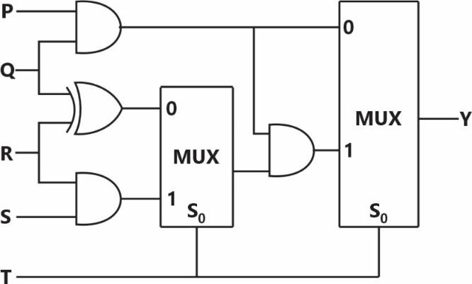
If all the inputs and are applied simultaneously and held constant, the maximum propagation delay of the circuit is


Sign in to see the solution
Log in to view the explanation, track your attempts, and keep your progress.
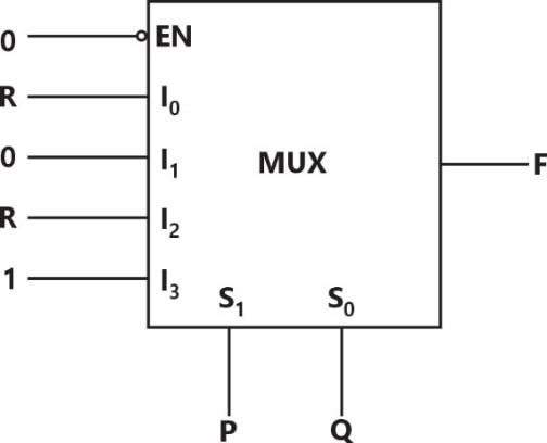
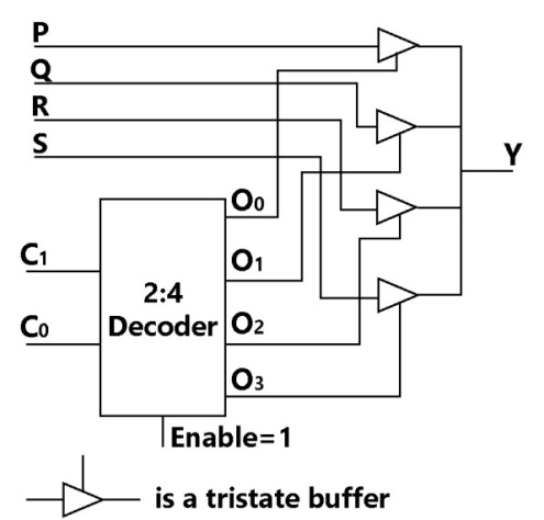
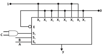
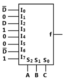
Sign in to UnlockThe figure below shows a multiplexer where and are the select lines. to are the input data lines, is the enable line, and is the output. is


Sign in to see the solution
Log in to view the explanation, track your attempts, and keep your progress.
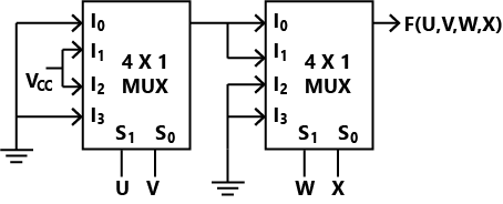
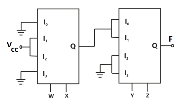
Sign in to UnlockA four-variable Boolean function is realized using multiplexers as shown in the figure. The minimized expression for is


Sign in to see the solution
Log in to view the explanation, track your attempts, and keep your progress.
Sign in to UnlockConsider the circuit shown in the figure.
The Boolean expression F implemented by the circuit is


Sign in to see the solution
Log in to view the explanation, track your attempts, and keep your progress.
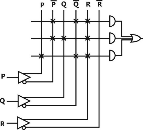
Sign in to UnlockA programmable logic array (PLA) is shown in the figure.


Sign in to see the solution
Log in to view the explanation, track your attempts, and keep your progress.
Sign in to UnlockFigure I shows a 4-bit ripple carry adder realized using full adders and Figure II shows the circuit of a full-adder (FA). The propagation delay of the XOR, AND and OR gates in Figure II are 20 ns. 15 ns and 10 ns. respectively. Assume all the inputs to the 4-bit adder are initially reset to 0.
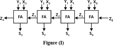
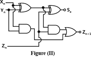
At t = 0, the inputs to the 4-bit adder are changed to


The output of the ripple carry adder will be stable at t (in ns) = _______________
Sign in to see the solution
Log in to view the explanation, track your attempts, and keep your progress.
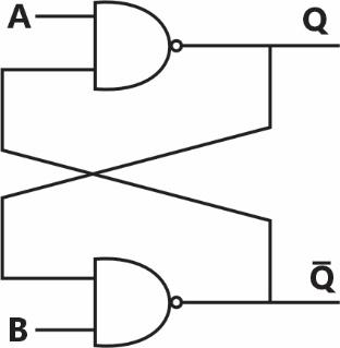
Sign in to UnlockIdentify the circuit below.
Sign in to see the solution
Log in to view the explanation, track your attempts, and keep your progress.
Sign in to UnlockThe functionality implemented by the circuit below is
Sign in to see the solution
Log in to view the explanation, track your attempts, and keep your progress.
Sign in to UnlockA 4:1 multiplexer is to be used for generating the output carry of a full adder. A and B are the bits to be added while is the input carry and is the output carry. A and B are to be used as the select bits with A being the more significant select bit.


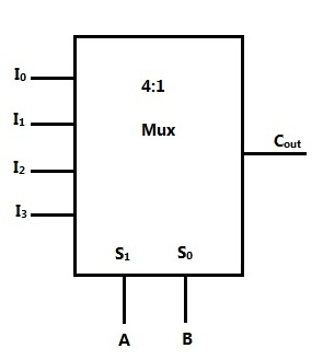
Which one of the following statements correctly describes the choice of signals to be connected to the inputs , , and so that the output is ?


, , and


,, and

, , and


, , and
Sign in to see the solution
Log in to view the explanation, track your attempts, and keep your progress.
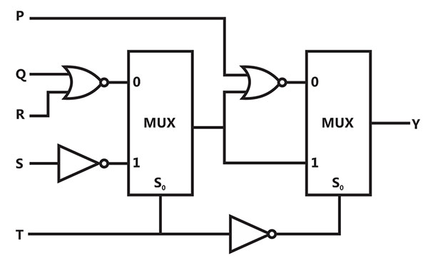
Sign in to UnlockFor the circuit shown in the figure, the delays of NOR gates, multiplexers and inverters are 2 ns, 1.5 ns and 1 ns, respectively. If all the inputs P, Q, R, S and T are applied at the same time instant, the maximum propagation delay (in ns) of the circuit is ___________
Sign in to see the solution
Log in to view the explanation, track your attempts, and keep your progress.
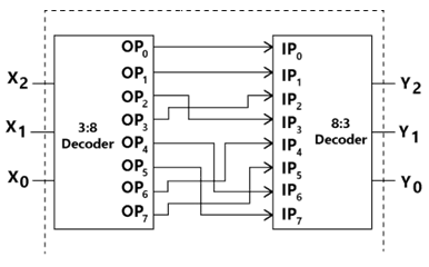
Sign in to UnlockA 1-to-8 de-multiplexer with data input , address inputs (with as the LSB) and and as the eight de-multiplexed outputs, is to be designed using two 2-to-4 decoders (with enable input and address inputs and ) as shown in the figure. and are to be connected to P, Q, R and S, but not necessarily in this order. The respective input connections to P, Q, R, and S terminals should be


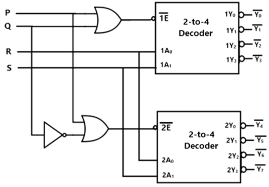


Sign in to see the solution
Log in to view the explanation, track your attempts, and keep your progress.
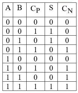
Sign in to UnlockIn a half-subtractor circuit with X and Y as inputs, the Borrow (M) and Difference (N = X - Y) are given by

,


,

,


Sign in to see the solution
Log in to view the explanation, track your attempts, and keep your progress.
Sign in to UnlockConsider the multiplexer-based logic circuit shown in the figure.
Which one of the following Boolean functions is realized by the circuit?


Sign in to see the solution
Log in to view the explanation, track your attempts, and keep your progress.
Sign in to UnlockIn the circuit shown, W and Y are MSBs of the control inputs. The output F is given by


Sign in to see the solution
Log in to view the explanation, track your attempts, and keep your progress.
Sign in to UnlockIf X and Y are inputs and the Difference (D = X – Y) and the Borrow (B) are the outputs, which one of the following diagrams implements a half-subtractor?
Sign in to see the solution
Log in to view the explanation, track your attempts, and keep your progress.
Sign in to UnlockAn 8-to-1 multiplexer is used to implement a logical function Y as shown in the figure. The output Y is given by


Sign in to see the solution
Log in to view the explanation, track your attempts, and keep your progress.
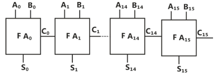
Sign in to UnlockA 16-bit ripple carry adder is realized using 16 identical full adders (FA) as shown in the figure. The carry-propagation delay of each FA is 12 ns and the sum-propagation delay of each FA is 15ns. The worst case delay (in ns) of this 16-bit adder will be __________.
Sign in to see the solution
Log in to view the explanation, track your attempts, and keep your progress.
Sign in to UnlockThe output Y of a 2-bit comparator is logic 1 whenever the 2-bit input A is greater than the 2-bit input B. The number of combinations for which the output is logic 1, is
Sign in to see the solution
Log in to view the explanation, track your attempts, and keep your progress.
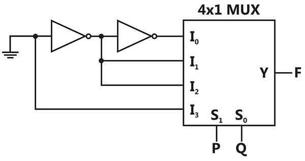
Sign in to UnlockThe logic function implemented by the circuit below is (ground implies a logic “0”)
Sign in to see the solution
Log in to view the explanation, track your attempts, and keep your progress.
Sign in to UnlockIn the circuit shown, the device connected to Y5 can have address in the range
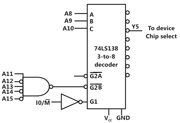
Sign in to see the solution
Log in to view the explanation, track your attempts, and keep your progress.
Sign in to UnlockThe Boolean function realized by the logic circuit shown is


Sign in to see the solution
Log in to view the explanation, track your attempts, and keep your progress.
Sign in to UnlockFor the circuit shown in the following figure, are inputs to the 4:1 multiplexer. R (MSB) and S are control bits. The output Z can be represented by

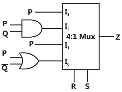
P Q + P S +


P + P Q +


P + Q R + P Q R S +

P Q + P Q R + P S +

Sign in to see the solution
Log in to view the explanation, track your attempts, and keep your progress.
Sign in to UnlockIn the following circuit, X is given by


Sign in to see the solution
Log in to view the explanation, track your attempts, and keep your progress.
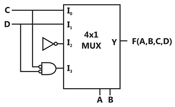
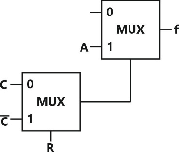
Sign in to UnlockThe Boolean function f implemented in the figure using two input multiplexers is


Sign in to see the solution
Log in to view the explanation, track your attempts, and keep your progress.
Sign in to UnlockThe minimum number of 2 to 1 multiplexers required to realize a 4 to 1 multiplexer is
Sign in to see the solution
Log in to view the explanation, track your attempts, and keep your progress.
Sign in to UnlockWithout any additional circuitry, an 8:1 MUX can be used to obtain
Sign in to see the solution
Log in to view the explanation, track your attempts, and keep your progress.
Sign in to UnlockThe circuit shown in figure has 4 boxes each described by inputs P, Q, R and outputs Y, Z with

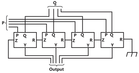

The circuit acts as a
Sign in to see the solution
Log in to view the explanation, track your attempts, and keep your progress.
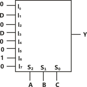
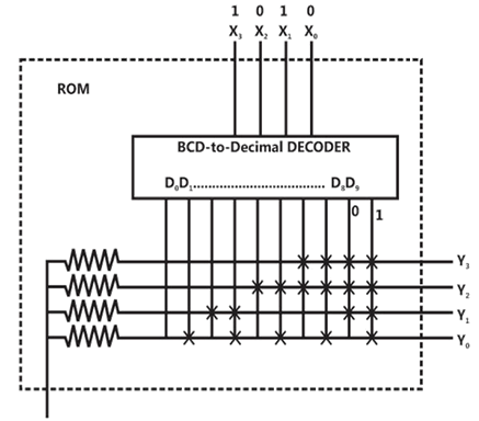
Sign in to UnlockIf the input to the ROM in figure are 8-4-2-1 BCD numbers, then the outputs are


Sign in to see the solution
Log in to view the explanation, track your attempts, and keep your progress.
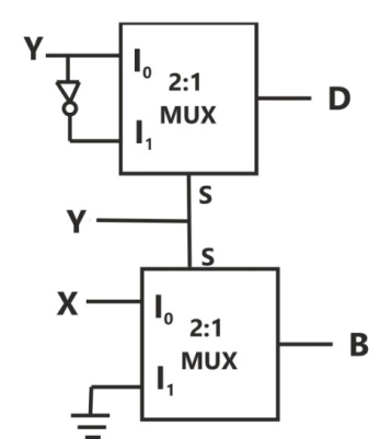
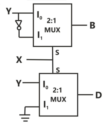
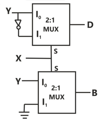
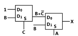
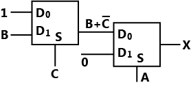
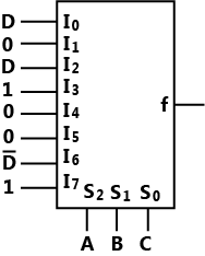
Sign in to UnlockThe inputs to a digital circuit shown in Figure are the external signals A, B and C.
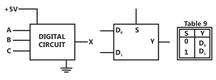
( and are not available. The +5V power supply (logic 1) and the ground (logic 0) are also available. The output of the circuit is .


(a) Write down the output function in its canonical SOP and POS forms.
(b) Implement the circuit using only two 2:1 multiplexers shown in Figures, where S is the data-select line, and are the input data lines and Y is the output lines. The function table for the multiplexer is given in table.


Canonical SOP form

Canonical POS form

Sign in to see the solution
Log in to view the explanation, track your attempts, and keep your progress.
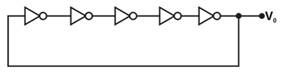
Sign in to UnlockFor the ring oscillator shown in the figure, the propagation delay of each inverter is 100pico second. What is the fundamental frequency of the oscillator output?
Sign in to see the solution
Log in to view the explanation, track your attempts, and keep your progress.
Sign in to UnlockIn the TTL circuit in figure, to are select lines and and are input lines. and are LSBs. The output Y is


Indeterminate


Sign in to see the solution
Log in to view the explanation, track your attempts, and keep your progress.
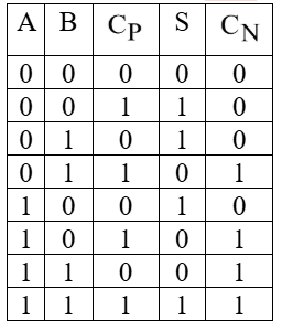
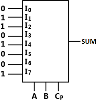
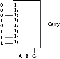
Sign in to UnlockA one-bit full adder is to be implemented using 8-to-1 multiplexers (MUX).
(a) Write the truth table for sum (S) and carry to the next stage in terms of the two bits (A, B) and carry from the previous stage , The truth table should be in the ascending order of , i.e. .


(b) Implement S and using 8-to-1 multiplexers.

Sign in to see the solution
Log in to view the explanation, track your attempts, and keep your progress.
Sign in to UnlockFor a binary half-sub-tractor having two inputs A and B, the correct set of logical expressions for the outputs D (=A minus B) and X (=borrow) are
,


,


,


,

Sign in to see the solution
Log in to view the explanation, track your attempts, and keep your progress.
Sign in to UnlockA 2-bit binary multiplier can be implemented using
Sign in to see the solution
Log in to view the explanation, track your attempts, and keep your progress.
Sign in to UnlockThe decoding circuit shown in the figure is has been used to generate the active low chip select signal for a microprocessor peripheral. (The address line are designated as AO to A7 for I/O addresses)
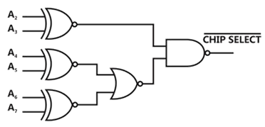
The peripheral will correspond to I/O addresses in the range
Sign in to see the solution
Log in to view the explanation, track your attempts, and keep your progress.
Sign in to UnlockA ring oscillator consisting of 5 inverters is running at a frequency of 1.0MHz. The propagation delay per gate is _________ n sec.
Sign in to see the solution
Log in to view the explanation, track your attempts, and keep your progress.
Sign in to UnlockThe look-ahead carry adder is a parallel carry adder where all sum digits are generated directly from the input digits. (True=1, False=0)
Sign in to see the solution
Log in to view the explanation, track your attempts, and keep your progress.
Sign in to UnlockSignals A, B, C, D and are available. Using a single 8 to 1 multiplexer and no other gate, implement the Boolean function


None of these
Sign in to see the solution
Log in to view the explanation, track your attempts, and keep your progress.
Sign in to UnlockThe logic realized by the circuit shown in figure is:
F = A.C

F = B.C

Sign in to see the solution
Log in to view the explanation, track your attempts, and keep your progress.
Sign in to UnlockA combinational circuit has three inputs, A, B and C and an output F.F. is true only for the following input combinations?
A is false and B is true
A is false and C is true
A, B and C are all false
A, B and C are all true
The truth table for F. use the convention, true = 1 and false = 0
Simplified expression for F as a sum of products.

Simplified expression for F as a product of sums.

logic circuit implementation of F using the minimum number of 2 input NAND gates only
Sign in to see the solution
Log in to view the explanation, track your attempts, and keep your progress.
Sign in to UnlockA sequential multiplexer is connected as shown in figure. Each time the multiplexer receives the clock, it switches to the next channel (From 6 it goes to 1). If the input signals are
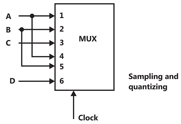
A =

B =

C =

D =

The minimum clock frequency should be _______ KHz.
Sign in to see the solution
Log in to view the explanation, track your attempts, and keep your progress.
Sign in to Unlock