Electronic Devices
PN Junction Theory
Practice questions from PN Junction Theory.
58
Total0
Attempted0
Correct0
IncorrectAn ideal p-n junction germanium diode has a reverse saturation current of at 300 K.

The voltage (in Volts, rounded off to two decimal places) to be applied across the junction to get a forward bias current of 100 mA at 300 K is _______.
(Consider the Boltzmann constant and the charge of an electron .)


Sign in to see the solution
Log in to view the explanation, track your attempts, and keep your progress.
Sign in to UnlockThe photocurrent of a PN junction diode solar cell is . The voltage corresponding to its maximum power point is . If the thermal voltage is , the reverse saturation current of the diode (in , rounded off to two decimal places) is______.


Sign in to see the solution
Log in to view the explanation, track your attempts, and keep your progress.
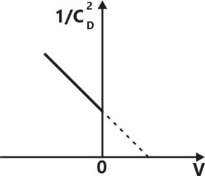
Sign in to UnlockA one-sided abrupt pn junction diode has a depletion capacitance of at a reverse bias of . The plot of versus the applied voltage for this diode is a straight line as shown in the figure below. The slope of the plot is __________ .


Sign in to see the solution
Log in to view the explanation, track your attempts, and keep your progress.
Sign in to UnlockA pn junction solar cell of area , illuminated uniformly with , has the following parameters: Efficiency , open circuit voltage , fill factor , and thickness , The charge of an electron is . The average optical generation rate (in ) is


Sign in to see the solution
Log in to view the explanation, track your attempts, and keep your progress.
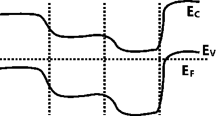
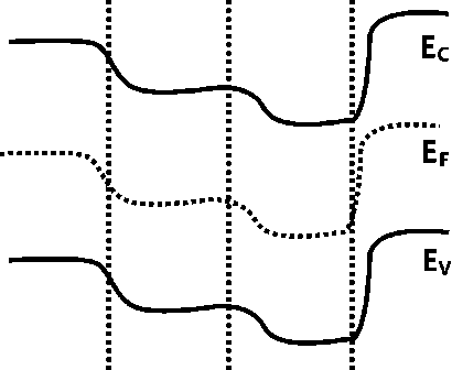
Sign in to UnlockWhich one of the following options describes correctly the equilibrium band diagram at T=300K of a Siliconconfiguration shown in the figure?


Sign in to see the solution
Log in to view the explanation, track your attempts, and keep your progress.
Sign in to UnlockIn an ideal pn junction with an ideality factor of 1 at T=300 K, the magnitude of the reverse-bias voltage required to reach 75% of its reverse saturation current, rounded off to 2 decimal places, is ___________mV.

Sign in to see the solution
Log in to view the explanation, track your attempts, and keep your progress.
Sign in to UnlockA p-n step junction diode with a contact potential of 0.65 V has a depletion width of 1 pm at equilibrium. The forward voltage (in volts. correct to two decimal places) at which this width reduces to is _______

Sign in to see the solution
Log in to view the explanation, track your attempts, and keep your progress.
Sign in to UnlockIn a p-n junction diode at equilibrium_ which one of the following statements is NOT TRUE?
Sign in to see the solution
Log in to view the explanation, track your attempts, and keep your progress.
Sign in to UnlockRed (R), Green (G) and Blue (b) Light Emitting Diodes (LEDs) were fabricated using p-n junctions of three different inorganic semiconductors having different band-gaps. The built-in voltages of red, green and blue diodes are and, respectively. Assume donor and acceptor doping to be the same (and, respectively) in the p and n sides of all the three diodes.


Which one of the following relationships about the built-in voltages is TRUE?


Sign in to see the solution
Log in to view the explanation, track your attempts, and keep your progress.
Sign in to UnlockAn Silicon device is fabricated with uniform and non-degenerate donor doping concentrations of and corresponding to the and n regions respectively. At the operational temperature T, assume complete impurity ionization, kT/q = 25 mV, and intrinsic carrier concentration to be . What is the magnitude of the built-in potential of this device?


Sign in to see the solution
Log in to view the explanation, track your attempts, and keep your progress.
Sign in to UnlockAs shown, two Silicon (Si) abrupt p-n unction diodes are fabricated with uniform donor doping concentrations of and in the n-regions of the diodes, and uniform acceptor doping concentrations of in the p-regions of the diodes, respectively. Assuming that the reverse bias voltage is built-in potentials of the diodes, the ratio of their reverse bias capacitances for the same applied reverse bias, is _________ .


Sign in to see the solution
Log in to view the explanation, track your attempts, and keep your progress.
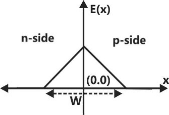
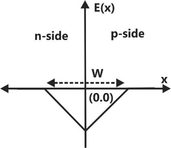
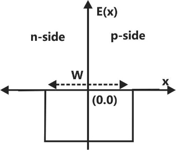
Sign in to UnlockAn abrupt pn junction (located at x = 0) is uniformly doped on both p and n sides. The width of the depletion region is W and the electric field variation in the x-direction is E(x). Which of the following figures represents the electric field profile near the pn junction?
Sign in to see the solution
Log in to view the explanation, track your attempts, and keep your progress.
Sign in to UnlockConsider a silicon p-n junction with a uniform acceptor doping concentration of on the p-side and a uniform donor doping concentration of on the n-side. No external voltage is applied to the diode. Given: kT/q = 26 mV, = 1.5 x , = , = 8.85 × and q = 1.6 × . The charge per unit junction area (nC ) in the depletion region on the p-side is__________


Sign in to see the solution
Log in to view the explanation, track your attempts, and keep your progress.
Sign in to UnlockConsider avalanche breakdown in a silicon junction. The n-region is uniformly doped with a donor density. Assume that breakdown occurs when the magnitude of the electric field at any point in the device becomes equal to the critical field . Assume to be independent of. If the built-in voltage of the junction is much smaller than the breakdown voltage, , the relationship between and is given by


= constant

= constant

= constant

= constant

Sign in to see the solution
Log in to view the explanation, track your attempts, and keep your progress.
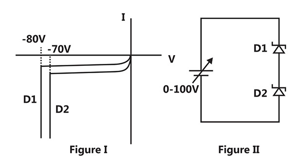
Sign in to UnlockThe I-V characteristics of the zener diodes D1 and D2 are shown in figure I. These diodes are used in the circuit given in figure II. If the supply voltage is varied from 0 to 100 V, then breakdown occurs
Sign in to see the solution
Log in to view the explanation, track your attempts, and keep your progress.
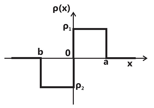
Sign in to UnlockConsider the charges profile shown in the figure. The resultant potential distribution is best described by
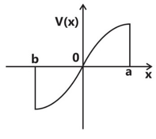
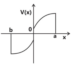
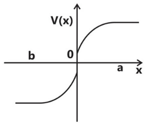
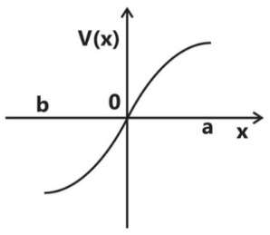
Sign in to see the solution
Log in to view the explanation, track your attempts, and keep your progress.
Sign in to UnlockA region of negative differential resistance is observed in the current voltage characteristics of a silicon PN junction if
Sign in to see the solution
Log in to view the explanation, track your attempts, and keep your progress.
Sign in to UnlockThe built-in potential of an abrupt p-n junction is 0.75 V. If its junction capacitance at a reverse bias of 1.25 V is 5 pF, the value of (in pF) when = 7.25 V is ________.


Sign in to see the solution
Log in to view the explanation, track your attempts, and keep your progress.
Sign in to UnlockFor a silicon diode with long P and N regions, the accepter and donor impurity concentrations are 1 × and 1 × , respectively. The lifetimes of electrons in P region and holes in N region are both 100 µs. The electron and hole diffusion coefficients are 49 and 36 , respectively. Assume kT/q = 26 mV, the intrinsic carrier concentration is 1 × , and q = 1.6 × C. When a forward voltage of 208 mV is applied across the diode, the hole current density (in nA/) injected from P region to N region is _____________.


Sign in to see the solution
Log in to view the explanation, track your attempts, and keep your progress.
Sign in to UnlockThe electric field profile in the depletion region of a p-n junction in equilibrium is shown in the figure. Which one of the following statements is NOT TRUE?
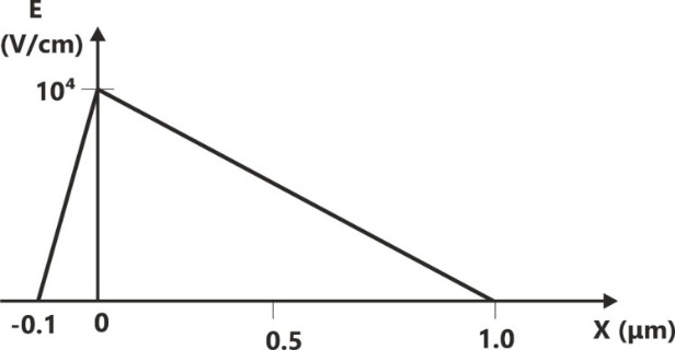
The left side of the junction is n-type and the right side is p-type
Both the n-type and p-type depletion regions are uniformly doped
The potential difference across the depletion region is 700 mV
If the p-type region has a doping concentration of , then the doping concentration in the n-type region will be
Sign in to see the solution
Log in to view the explanation, track your attempts, and keep your progress.
Sign in to UnlockThe doping concentrations on the p-side and n-side of a silicon diode are and , respectively. A forward bias of 0.3 V is applied to the diode. At T = 300 K, the intrinsic carrier concentration of silicon and . The electron concentration at the edge of the depletion region on the p-side is


Sign in to see the solution
Log in to view the explanation, track your attempts, and keep your progress.
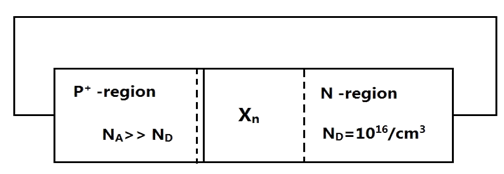
Sign in to UnlockConsider an abrupt PN junction (at T = 300 K) shown in the figure. The depletion region width on the N-side of the junction is 0.2 µm and the permittivity of silicon () is . At the junction, the approximate value of the peak electric field (in kV/cm) is _________.


Sign in to see the solution
Log in to view the explanation, track your attempts, and keep your progress.
Sign in to UnlockWhen a silicon diode having a doping concentration of on p-side and on n-side is reverse biased, the total depletion width is found to be 3 µm. Given that the permittivity of silicon is , the depletion width on the p-side and the maximum electric field in the depletion region, respectively, are


2.7 µm and

0.3 µm and

0.3 µm and

2.1 µm and
Sign in to see the solution
Log in to view the explanation, track your attempts, and keep your progress.
Sign in to UnlockThe donor and accepter impurities in an abrupt junction silicon diode are and , respectively. Assume that the intrinsic carrier concentration in silicon at 300 K, and the permittivity of silicon . The built-in potential and the depletion width of the diode under thermal equilibrium conditions, respectively, are


0.7 V and

0.86 V and
0.7 V and

0.86 V and
Sign in to see the solution
Log in to view the explanation, track your attempts, and keep your progress.
Sign in to UnlockIn a forward biased pn junction diode, the sequence of events that best describes the mechanism of current flow is
Sign in to see the solution
Log in to view the explanation, track your attempts, and keep your progress.
Sign in to UnlockA silicon PN junction is forward biased with a constant current at room temperature. When the temperature is increased by , the forward bias voltage across the PN junction

Sign in to see the solution
Log in to view the explanation, track your attempts, and keep your progress.
Sign in to UnlockA Zener diode, when used in voltage stabilization circuits, is biased in
Sign in to see the solution
Log in to view the explanation, track your attempts, and keep your progress.
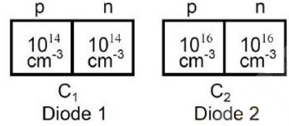
Sign in to UnlockCompared to a p-n junction with , which one of the following statements is TRUE for a p-n junction with ?


Sign in to see the solution
Log in to view the explanation, track your attempts, and keep your progress.
Sign in to UnlockConsider a silicon p-n junction at room temperature having the following parameters:
Doping on the n-side

Depletion width on the n-side

Depletion width on the p-side

Intrinsic carrier concentration

Thermal voltage = 26 mV
Permittivity of free space

Dielectric constant of silicon = 12
The built-in-potential of the junction
Sign in to see the solution
Log in to view the explanation, track your attempts, and keep your progress.
Sign in to UnlockConsider a silicon p-n junction at room temperature having the following parameters:
Doping on the n-side
Depletion width on the n-side
Depletion width on the p-side
Intrinsic carrier concentration
Thermal voltage = 26 mV
Permittivity of free space
Dielectric constant of silicon = 12
The peak electric field in the device is
, directed from p-region to n-region

, directed from n-region to p-region
, directed from p-region to n-region

, directed from n-region to p-region
Sign in to see the solution
Log in to view the explanation, track your attempts, and keep your progress.
Sign in to UnlockWhich of the following is NOT associated with a p-n junction?
Sign in to see the solution
Log in to view the explanation, track your attempts, and keep your progress.
Sign in to UnlockConsider the following assertions.
S1: For Zener effect to occur, a very abrupt junction is required.
S2: For quantum tunnelling to occur, a very narrow energy barrier is required.
Which of the following is correct?
Sign in to see the solution
Log in to view the explanation, track your attempts, and keep your progress.
Sign in to UnlockIn a n junction diode under reverse bias, the magnitude of electric field is maximum at

The edge of the depletion region on the p-side
The edge of the depletion region on the n-side
The n junction
The centre of the depletion region on the n-side
Sign in to see the solution
Log in to view the explanation, track your attempts, and keep your progress.
Sign in to UnlockA junction has a built-in potential of 0.8 V. The depletion layer width at a reverse bias of 1.2V is 2μm. For a reverse bias of 7.2V, the depletion layer width will be
Sign in to see the solution
Log in to view the explanation, track your attempts, and keep your progress.
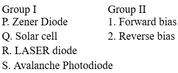
Sign in to UnlockGroup I lists four types of p-n junction diodes. Match each device in Group I with one of the options in Group II to indicate the bias condition of that device in its normal mode of operation.
Sign in to see the solution
Log in to view the explanation, track your attempts, and keep your progress.
Sign in to UnlockThe values of voltage across a tunnel-diode corresponding to peak and valley currents are and respectively. The range of tunnel-diode voltage for which the slope of its characteristics is negative would be


Sign in to see the solution
Log in to view the explanation, track your attempts, and keep your progress.
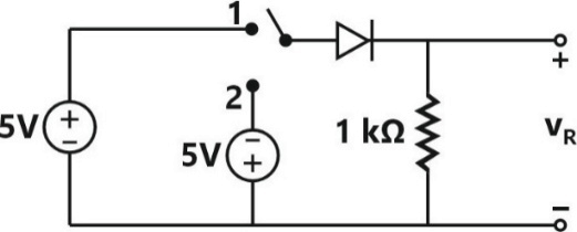
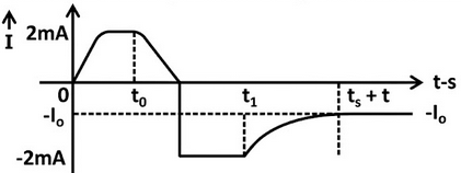
Sign in to UnlockIn the circuit shown below, the switch was connected to position 1 at t < 0 and at t = 0, it is changed to position 2. Assume that the diode has zero voltage drop and a storage time. For,is given by (all in Volts)


Sign in to see the solution
Log in to view the explanation, track your attempts, and keep your progress.
Sign in to UnlockFind the correct match between Group 1 and Group 2:
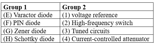
Sign in to see the solution
Log in to view the explanation, track your attempts, and keep your progress.
Sign in to UnlockA silicon PN junction at a temperature of has a reverse saturation current of 10 pico-Amperes (pA).

The reverse saturation current at for the same bias is approximately

Sign in to see the solution
Log in to view the explanation, track your attempts, and keep your progress.
Sign in to UnlockA silicon PN junction diode under reverse bias has depletion region of width, the relative permittivity of silicon, and the permittivity of free space. The depletion capacitance of the diode per square meter is


Sign in to see the solution
Log in to view the explanation, track your attempts, and keep your progress.
Sign in to UnlockIn an abrupt p-n junction, the doping concentrations on the p-side and n-side are and respectively. The p-n junction is reserve biased and the total depletion width is 3μm. The depletion width on the p-side is


Sign in to see the solution
Log in to view the explanation, track your attempts, and keep your progress.
Sign in to UnlockConsider an abrupt p-junction. Let be the built-in potential of this junction and be the applied reverse bias. If the junction capacitance is 1 pF for , then for , will be


Sign in to see the solution
Log in to view the explanation, track your attempts, and keep your progress.
Sign in to UnlockChoose proper substitutes for X and Y to make the following statement correct Tunnel diode and Avalanche photodiode are operated in X bias and Y bias respectively.
Sign in to see the solution
Log in to view the explanation, track your attempts, and keep your progress.
Sign in to UnlockMatch items in Group 1 with items in Group 2, most suitably
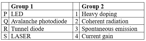
Sign in to see the solution
Log in to view the explanation, track your attempts, and keep your progress.
Sign in to UnlockAt 300 K, for a diode current of 1mA, a certain germanium diode requires a forward bias of 0.1435V, whereas a certain silicon diode requires a forward bias of 0.718V. Under the conditions stated above, the closest approximation of the ratio of reverse saturation current in germanium diode to that in silicon diode is
1
5


Sign in to see the solution
Log in to view the explanation, track your attempts, and keep your progress.
Sign in to UnlockA particular green LED emits light of wavelength 5490ºA. The energy band-gap of the semiconductor material used there is
(Plank’s constant =)

Sign in to see the solution
Log in to view the explanation, track your attempts, and keep your progress.
Sign in to UnlockIn Figure a silicon diode is carrying a constant current of 1 mA. When the temperature of the diode is 20ºC, is found to be 700 mV. If the temperature rises to 40ºC, becomes approximately equal to
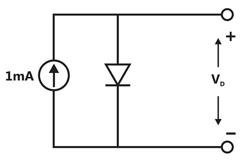
Sign in to see the solution
Log in to view the explanation, track your attempts, and keep your progress.
Sign in to UnlockThe static characteristic of an adequately forward biased p-n junction is a straight line, if the plot is of
Sign in to see the solution
Log in to view the explanation, track your attempts, and keep your progress.
Sign in to UnlockThe p-type substrate in a conventional pn-junction isolated integrated circuit should be connected to
Sign in to see the solution
Log in to view the explanation, track your attempts, and keep your progress.
Sign in to UnlockThe diffusion potential across a P-N junction
Sign in to see the solution
Log in to view the explanation, track your attempts, and keep your progress.
Sign in to UnlockA zener diode works on the principle of
Sign in to see the solution
Log in to view the explanation, track your attempts, and keep your progress.
Sign in to UnlockThe depletion capacitance, , of an abrupt P-N junction with constant doping on either side varies with reverse bias, , as


Sign in to see the solution
Log in to view the explanation, track your attempts, and keep your progress.
Sign in to UnlockThe built-in potential (Diffusion potential) in a p-n junction
Sign in to see the solution
Log in to view the explanation, track your attempts, and keep your progress.
Sign in to UnlockA P-N junction in series with a 100 ohms resistor is forward biased so that a current of 100mA flows. If the voltage across this combination is instantaneously reversed to 10 V at, the reverse current that flows through the diode at is approximately given by

Sign in to see the solution
Log in to view the explanation, track your attempts, and keep your progress.
Sign in to UnlockAn infrared LED is usually fabricated from
Sign in to see the solution
Log in to view the explanation, track your attempts, and keep your progress.
Sign in to UnlockThe small signal capacitances of an abrupt junction is at zero bias. If the built in voltage is 1 volt, the capacitance at a reverse bias voltage of 99 volts is equal to __


Sign in to see the solution
Log in to view the explanation, track your attempts, and keep your progress.
Sign in to UnlockReferring to the figure. The switch S is in position 1 initially and steady state conditions exist from time to . The switch is suddenly thrown into position 2. The current I through the 10K resistor as a function of time t from , is ….. (Give the sketch showing the magnitudes of the current at , and )


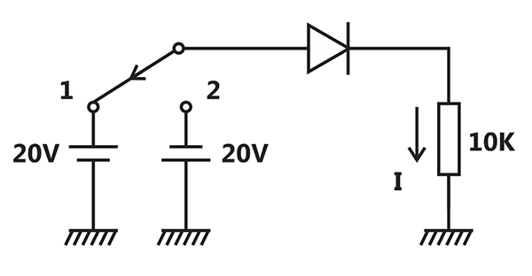
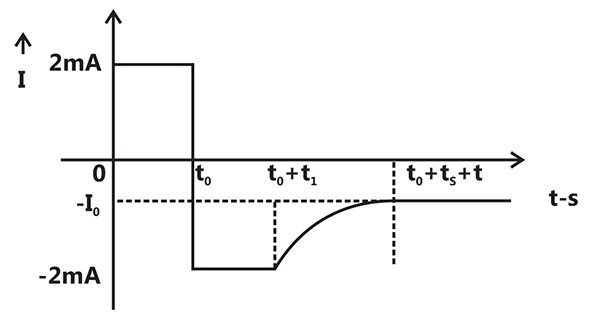
Sign in to see the solution
Log in to view the explanation, track your attempts, and keep your progress.
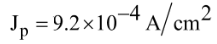
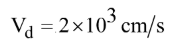
Sign in to UnlockThe current I in a forward biased junction shown in figure (a) is entirely due to diffusion of holes from and . The injected hole concentration distribution in the n-region is linear as shown in figure (b), with and .


Determine:
(a) The current density in the diode, assuming that the diffusion coefficient of holes is

(b) The velocity of holes in the n-region at.
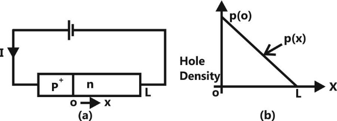
(a)

(b)

(a)
(b)
Sign in to see the solution
Log in to view the explanation, track your attempts, and keep your progress.
Sign in to Unlock