Electronic Devices
Fabrication
Practice questions from Fabrication.
7
Total0
Attempted0
Correct0
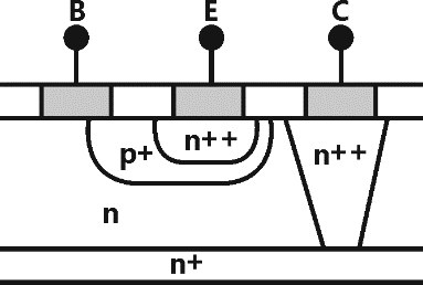
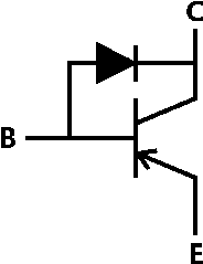
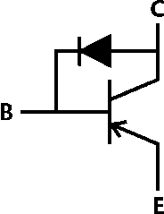
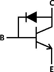
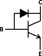
IncorrectThe correct circuit representation of the structure shown in the figure is
Sign in to see the solution
Log in to view the explanation, track your attempts, and keep your progress.
Sign in to UnlockThere are two photolithography systems: one with light source of wavelength (System 1) and another with light source of wavelength (System 2). Both photolithography systems are otherwise identical. If the minimum feature sizes that can be realized using System1 and System2 are and respectively, the ratio (correct to two decimal places) is





Sign in to see the solution
Log in to view the explanation, track your attempts, and keep your progress.
Sign in to UnlockWhich one of the following processes is preferred to form the gate dielectric of MOSFETs?

Sign in to see the solution
Log in to view the explanation, track your attempts, and keep your progress.
Sign in to UnlockIn CMOS technology, shallow P-well or N-well regions can be formed using
Sign in to see the solution
Log in to view the explanation, track your attempts, and keep your progress.
Sign in to UnlockIn IC technology, dry oxidation (using dry oxygen) as compared to wet oxidation (using steam or water vapor) produces
Sign in to see the solution
Log in to view the explanation, track your attempts, and keep your progress.
Sign in to UnlockA silicon wafer has of oxide on it and is inserted in a furnace at a temperature above for further oxidation in dry oxygen. The oxidation rate


Sign in to see the solution
Log in to view the explanation, track your attempts, and keep your progress.
Sign in to UnlockIf P is Passivation, Q is n-well implant, R is metallization and S is source/drain diffusion, then the order in which they are carried out in a standard n-well CMOS fabrication process, is
Sign in to see the solution
Log in to view the explanation, track your attempts, and keep your progress.
Sign in to Unlock