Electronic Devices
BJT
Practice questions from BJT.
26
Total0
Attempted0
Correct0
IncorrectWhich of the following statements is/are true for a BJT with respect to its DC current gain ?

Under high-level injection condition in forward active mode, will decrease with increase in the magnitude of collector current.
Under low-level injection condition in forward active mode, where the current at the emitter-base junction is dominated by recombination-generation process, will decrease with increase in the magnitude of collector current.
will be lower when the BJT is in saturation region compared to when it is in active region.
A higher value of will lead to a lower value of the collector-to-emitter breakdown voltage.
Sign in to see the solution
Log in to view the explanation, track your attempts, and keep your progress.
Sign in to UnlockThe base of an npn BJT T1 has a linear doping profile as shown below. The base of another npn BJT T2 has a uniform doping of . All other parameters are identical for both the devices. Assuming that the hole density profile is the same as that of doping, the common-emitter current gain of T2 is



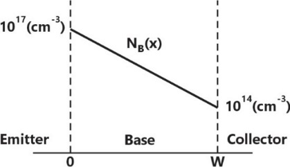
approximately 0.3 times that of

approximately 0.7 times that of
approximately 2.5 times that of
None of These
Sign in to see the solution
Log in to view the explanation, track your attempts, and keep your progress.
Sign in to UnlockFor a narrow base PNP BJT, the excess minority carrier concentrations (for emitter, for base, for collector) normalized to equilibrium minority carrier concentrations (for emitter,for base, for collector) in the quasi-neutral emitter, base and collector regions are shown below. Which one of the following biasing modes is the transistor operating in?






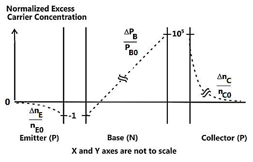
Sign in to see the solution
Log in to view the explanation, track your attempts, and keep your progress.
Sign in to UnlockThe Ebers-Moll model of a BJT is valid
Sign in to see the solution
Log in to view the explanation, track your attempts, and keep your progress.
Sign in to UnlockThe injected excess electron concentration profile in the base region of an NPN BJT, biased in the active region, is linear, as shown in the figure. If the area of the emitter-base junction is 0.001 , = 800 in the base region and depletion layer widths are negligible, then the collector current (in mA) at room temperature is ____________




(Given: thermal voltage = 26 mV at room temperature, electronic charge q=1.6 × C)


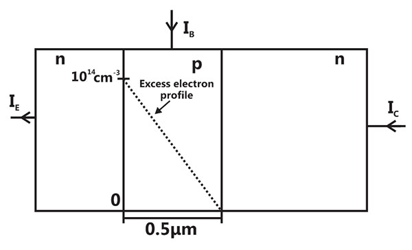
Sign in to see the solution
Log in to view the explanation, track your attempts, and keep your progress.
Sign in to UnlockIf the base width in a bipolar junction transistor is doubled, which one of the following statements will be TRUE?
Sign in to see the solution
Log in to view the explanation, track your attempts, and keep your progress.
Sign in to UnlockAn NPN BJT having reverse saturation current is biased in the forward active region with = 700 mV. The thermal voltage () is 25 mV and the current gain (β) may vary from 50 to 150 due to manufacturing variations. The maximum emitter current (in µA) is ________.


Sign in to see the solution
Log in to view the explanation, track your attempts, and keep your progress.
Sign in to UnlockAn increase in the base recombination of a BJT will increase
The common emitter dc current gain β
The breakdown voltage

The unity-gain cut-off frequency

The transconductance

Sign in to see the solution
Log in to view the explanation, track your attempts, and keep your progress.
Sign in to UnlockConsider two BJTs biased at the same collector current with area = 0.2 µm × 0.2 µm and = 300 µm × 300 µm. Assuming that all other device parameters are identical, kT/q = 26 mV, the intrinsic carrier concentration is 1 × , and q = 1.6 × C, the difference between the base-emitter voltages (in mV) of the two BJTs is _____.





Sign in to see the solution
Log in to view the explanation, track your attempts, and keep your progress.
Sign in to UnlockIn a uniformly doped BJT, assume that , and are the emitter, base and collector dopings in , respectively. If the emitter injection efficiency of the BJT is close unity, which one of the following conditions is TRUE?








Sign in to see the solution
Log in to view the explanation, track your attempts, and keep your progress.
Sign in to UnlockThe DC current gain (β) of a BJT is 50. Assuming that the emitter injection efficiency is 0.995, the base transport factor is
Sign in to see the solution
Log in to view the explanation, track your attempts, and keep your progress.
Sign in to UnlockThe phenomenon known as “Early Effect” in a bipolar transistor refers to a reduction of the effective base-width caused by
Sign in to see the solution
Log in to view the explanation, track your attempts, and keep your progress.
Sign in to UnlockIf for a silicon n-p-n transistor, the base-to-emitter voltage is 0.7V and the collector-to-base voltage is 0.2V, then the transistor is operating in the


Sign in to see the solution
Log in to view the explanation, track your attempts, and keep your progress.
Sign in to UnlockConsider the following statements and .


: The β of a bipolar transistor reduces if the base width is increased.
: The β of a bipolar transistor increases if the doping concentration in the base in increased.
Which one of the following is correct?
is FALSE and is TRUE
both and are TRUE
both and are FALSE
is TRUE and is FALSE
Sign in to see the solution
Log in to view the explanation, track your attempts, and keep your progress.
Sign in to UnlockThe neutral base width of a bipolar transistor, biased in the active region, is 0.5 μm. The maximum electron concentration and the diffusion constant in the base are and respectively. Assuming negligible recombination in the base, the collector current density (the electron charge is coulomb)



800

8
200
2
Sign in to see the solution
Log in to view the explanation, track your attempts, and keep your progress.
Sign in to UnlockThe early effect in a bipolar junction transistor is caused by
Sign in to see the solution
Log in to view the explanation, track your attempts, and keep your progress.
Sign in to UnlockIn a common emitter BJT amplifier, the maximum usable supply voltage is limited by
Avalanche breakdown of Base-Emitter junction
Collector-Base breakdown voltage with emitter open

Collector-Emitter breakdown voltage with base open

Zener breakdown voltage of the Emitter-Base junction
Sign in to see the solution
Log in to view the explanation, track your attempts, and keep your progress.
Sign in to UnlockFor a typical n-p-n transistor, as shown in the figure we have the following data available
and Collector doping
and Emitter doping
Minority carrier life time in the Base region is






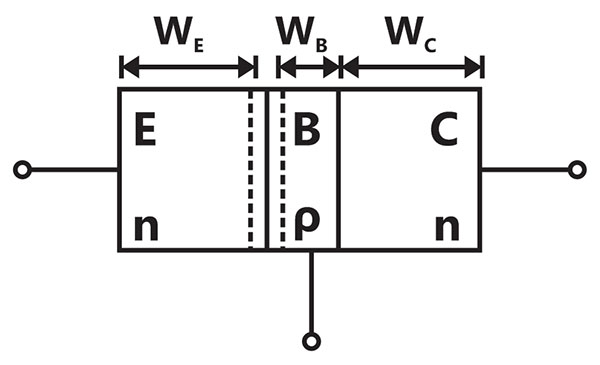
Under Punch-through condition the volts.

Here is the built in potential of Base-collector junction. Emitter Injection efficiency can be assumed as 1 for this transistor.

Evaluate Base Width and the current gain . [Standard data for this question is: coulombs; .




For silicon at, ; ; ]






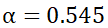
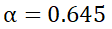
Sign in to see the solution
Log in to view the explanation, track your attempts, and keep your progress.
Sign in to UnlockIf a transistor is operating with both of its junctions forward biased, but with the collector base forward bias greater than the emitter – base forward bias, then it is operating in the
Sign in to see the solution
Log in to view the explanation, track your attempts, and keep your progress.
Sign in to UnlockThe common-emitter short circuit current gain of a transistor

Is a monotonically increasing function of the collector current

Is a monotonically decreasing function of
Increases with, for low, reaches a maximum and then decreases with further increase in
Is not a function of
Sign in to see the solution
Log in to view the explanation, track your attempts, and keep your progress.
Sign in to UnlockIn a bipolar transistor at room temperature, if the emitter current is doubled the voltage across its base-emitter junction
Sign in to see the solution
Log in to view the explanation, track your attempts, and keep your progress.
Sign in to UnlockThe break down voltage of a transistor with its base open is and that with emitter open is then,





is not related to
Sign in to see the solution
Log in to view the explanation, track your attempts, and keep your progress.
Sign in to UnlockA BJT is said to be operating in the saturation region of
Sign in to see the solution
Log in to view the explanation, track your attempts, and keep your progress.
Sign in to Unlock- cut off frequency of a bipolar junction transistor
Sign in to see the solution
Log in to view the explanation, track your attempts, and keep your progress.
Sign in to UnlockIn a transistor having finite β, the forward bias across the base emitter junction is kept constant and the reverse bias across the collector base junction is increased. Neglecting the leakage across the collector base junction and the depletion region generating current, the base current will __________.
Sign in to see the solution
Log in to view the explanation, track your attempts, and keep your progress.
Sign in to UnlockA P-N-P transistor shown in the figure has uniform doping in the emitter, base and collector regions, where in the doping concentrations are per , per , per , respectively. The minority carrier diffusion lengths in the emitter and the base regions are 5 microns and 100 microns, respectively. Assuming low level injection conditions and using the law of the junction, calculate the collector current density and the base current density and the base current density due to base recombination. [Suitable approximations may be made if required]. In all the regions of the transistors per sec per sec, per , KT/q=26 mV,









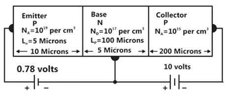
Collector Current Density
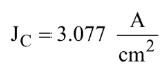
Base Current Density
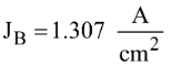
Base Current Density due to base recombination
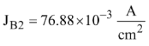
None
Sign in to see the solution
Log in to view the explanation, track your attempts, and keep your progress.
Sign in to Unlock