Digital Electronics
Sequential Circuits
Practice questions from Sequential Circuits.
78
Total0
Attempted0
Correct0
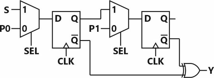
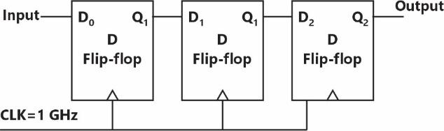
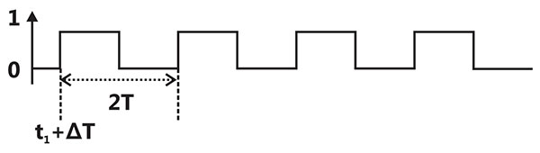
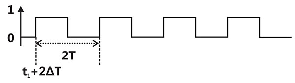
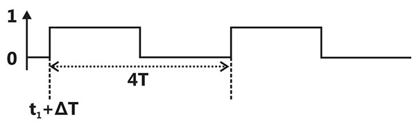
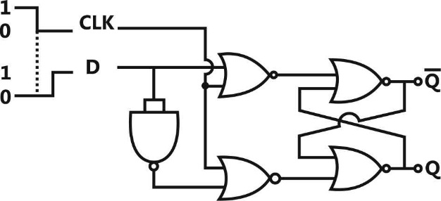
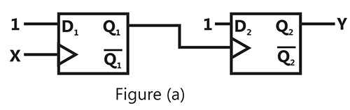
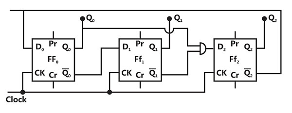
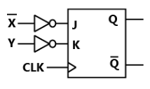
IncorrectA positive-edge-triggered sequential circuit is shown below. There are no timing violations in the circuit. Input is set to logic ' 0 ' and is set to logic ' 1 ' at all times. The timing diagram of the inputs and are also shown below.


The sequence of output from time to is ________.


Sign in to see the solution
Log in to view the explanation, track your attempts, and keep your progress.
Sign in to UnlockIn the circuit shown below, the AND gate has a propagation delay of 1 ns. The edge-triggered flip-flops have a set-up time of 2 ns, a hold-time of 0 ns, and a clock-to-Q delay of 2 ns.
The maximum clock frequency (in MHz, rounded off to the nearest integer) such that there are no setup violations is ________
Sign in to see the solution
Log in to view the explanation, track your attempts, and keep your progress.
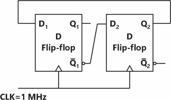
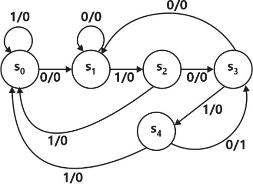
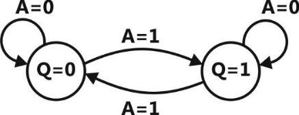
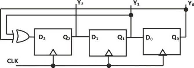
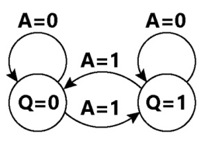
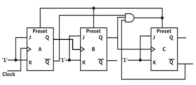
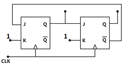
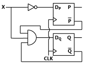
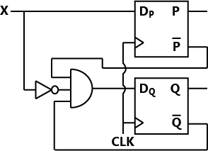
Sign in to UnlockThe sequence of states of the given synchronous sequential circuit is ________.


Sign in to see the solution
Log in to view the explanation, track your attempts, and keep your progress.
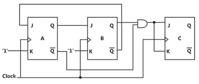
Sign in to UnlockThe synchronous sequential circuit shown below works at a clock frequency of . The throughput, in bits/s, and the latency, in ns, respectively, are


1000,3

2000,3

Sign in to see the solution
Log in to view the explanation, track your attempts, and keep your progress.
Sign in to UnlockIn a given sequential circuit, initial states are and . For a clock frequency of , the frequency of signal in , is ________. (rounded off to the nearest integer).


Sign in to see the solution
Log in to view the explanation, track your attempts, and keep your progress.
Sign in to UnlockFor the circuit shown, the clock frequency is and the duty cycle is . For the signal at the output of the Flip-Flop, ________.


frequency is and duty cycle is 50%

frequency is and duty cycle is
frequency is and duty cycle is


frequency is and duty cycle is
Sign in to see the solution
Log in to view the explanation, track your attempts, and keep your progress.
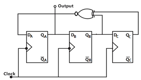
Sign in to UnlockThe propagation delay of the exclusive-OR (XOR) gate in the circuit in the figure is . The propagation delay of all the flip-flops is assumed to be zero. The clock (Clk) frequency provided to the circuit is .


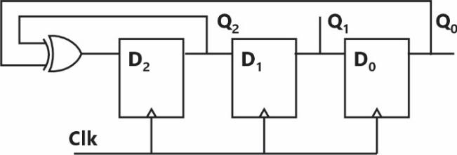
Starting from the initial value of the flip-flop outputs with , the minimum number of triggering clock edges after which the flip-flop outputs becomes 100 (in integer) is _________.


Sign in to see the solution
Log in to view the explanation, track your attempts, and keep your progress.
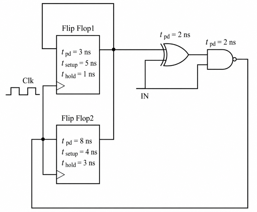
Sign in to UnlockFor the components in the sequential circuit shown below, $\scriptstyle t_{pd}$ is the propagation delay, $\scriptstyle t_{setup}$ is the setup time, and $\scriptstyle t_{hold}$ is the hold time. The maximum clock frequency (rounded off to the nearest integer), at which the given circuit can operate reliably, is __________ MHz.
Sign in to see the solution
Log in to view the explanation, track your attempts, and keep your progress.
Sign in to UnlockThe state diagram of a sequence detector is shown below. State is the initial state of the sequence detector. If the output is 1, then

Sign in to see the solution
Log in to view the explanation, track your attempts, and keep your progress.
Sign in to Unlockn the circuit shown, the clock frequency, i.e., the frequency of the CLK signal is 12 kHz. The frequency of the signal atis _______kHz

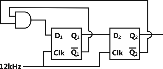
Sign in to see the solution
Log in to view the explanation, track your attempts, and keep your progress.
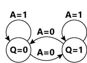
Sign in to UnlockThe state transition diagram for the circuit shown is
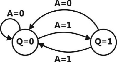
Sign in to see the solution
Log in to view the explanation, track your attempts, and keep your progress.
Sign in to UnlockA traffic signal cycles from GREEN to YELLOW. YELLOW to RED and RED to GREEN. In each cycle, GREEN is turned on for 70 seconds, YELLOW is turned on for 5 seconds and the RED is turned on for 75 seconds. This traffic light has to be implemented using a finite state machine (FSM). The only input to this FSM is a clock of 5 second period. The minimum number of flip-flops required to implement this FSM is _
Sign in to see the solution
Log in to view the explanation, track your attempts, and keep your progress.
Sign in to UnlockIn the circuit shown below, a positive edge-triggered D Flip-Flop is used for sampling input data using clock CK. The XOR gate outputs 3.3 volts for logic HIGH and 0 volts for logic LOW levels. The data bit and clock periods are equal and the valise of
, where the parameters and are shown m the figure. Assume that the Flip-Flop and the XOR gate are ideal.


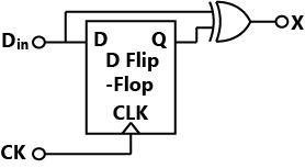
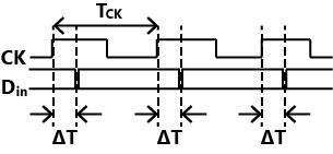
If the probability of input data bit transition in each clock period is 0.3, the average value (m volts, accurate to two decimal places) of the voltage at node X, is _______

Sign in to see the solution
Log in to view the explanation, track your attempts, and keep your progress.
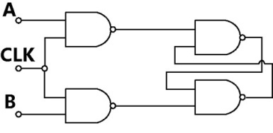
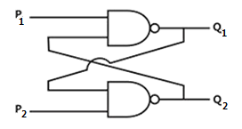
Sign in to UnlockIn the latch circuit shown, the NAND gates have non-zero, but unequal propagation delays. The present input condition is: P = Q = ‘0’. If the input condition is changed simultaneously to P = Q = ‘1’, the outputs X and Y are
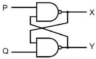

either

either


Sign in to see the solution
Log in to view the explanation, track your attempts, and keep your progress.
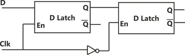
Sign in to UnlockConsider the D-Latch shown in the figure, which is transparent when its clock input CK is high and has zero propagation delay. In the figure, the clock signal CLK1 has a 50% duty cycle and CLK2 is a one-fifth period delayed version of CLK1. The duty cycle at the output of the latch in percentage is __
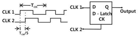
Sign in to see the solution
Log in to view the explanation, track your attempts, and keep your progress.
Sign in to UnlockA 4-bit shift register circuit configured for right-shift operation, i.e. is shown. If the present state of the shift register is ABCD = 1101, the number of clock cycles required to reach the state ABCD = 1111 is ___________ .

Sign in to see the solution
Log in to view the explanation, track your attempts, and keep your progress.
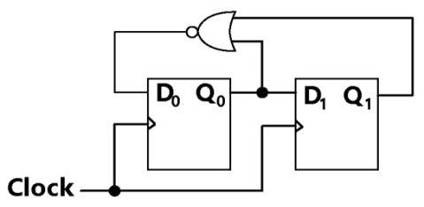
Sign in to UnlockA finite state machine (FSM) is implemented using the D flip-flops A and B, and logic gates, as shown in the figure below. The four possible states of the FSM are

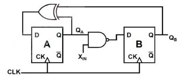
Assume that is held at a constant logic level throughout the operation of the FSM. When the FSM is initialized to the state and clocked, after a few clock cycles, it starts cycling through


all of the four possible states if

three of the four possible state if

only two of the four possible states if
only two of the four possible states if
Sign in to see the solution
Log in to view the explanation, track your attempts, and keep your progress.
Sign in to UnlockThe state diagram of a finite state machine (FSM) designed to detect an overlapping sequence of three bits is shown in figure. The FSM has an input ‘In’ and an output ‘Out’. The initial state of the FSM is .
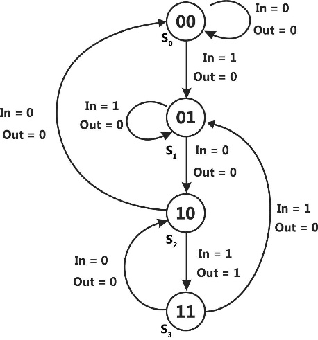
If the input sequence is 10101101001101, starting with the left-most bit, then the number of times will be 1 is ____
Sign in to see the solution
Log in to view the explanation, track your attempts, and keep your progress.
Sign in to UnlockAssume that all the digital gates in the circuit shown in the figure are ideal, the resistor and the supply voltage is 5V. The D flip-flops ,,, and are initialized with logic values 0,1,0,1 and 0, respectively. The clock has a 30% duty cycle.


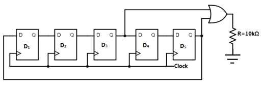
The average power dissipated (in mW) in the resistor R is ________.
Sign in to see the solution
Log in to view the explanation, track your attempts, and keep your progress.
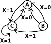
Sign in to UnlockThe state transition diagram for a finite state machine with states A, B and C, and binary inputs X, Y and Z, is shown in the figure.
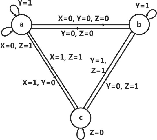
Which one of the following statements is correct?
Sign in to see the solution
Log in to view the explanation, track your attempts, and keep your progress.
Sign in to UnlockFor the circuit shown in the figure, the delay of the bubbled NAND gate is 2 ns and that of the counter is assumed to be zero.
If the clock (CLK) frequency is 1 GHz, then the counter behaves as a
Sign in to see the solution
Log in to view the explanation, track your attempts, and keep your progress.
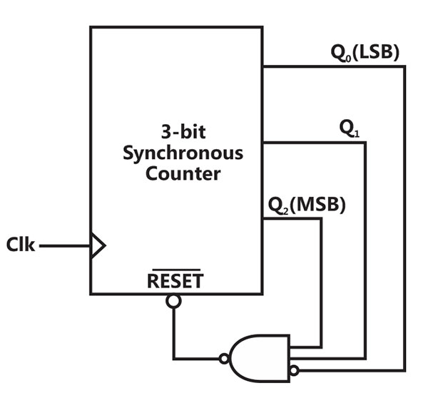
Sign in to UnlockA mod-n counter using a synchronous binary up-counter with synchronous clear input is shown in the figure. The value of n is _______
Sign in to see the solution
Log in to view the explanation, track your attempts, and keep your progress.
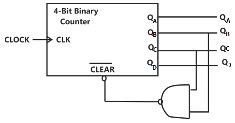
Sign in to UnlockThe figure shows a binary counter with synchronous clear input. With the decoding logic shown, the counter works as a
Sign in to see the solution
Log in to view the explanation, track your attempts, and keep your progress.
Sign in to UnlockThe circuit shown consists of J-K flip-flops, each with an active low asynchronous reset (input). The counter corresponding to this circuit is

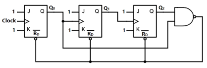
Sign in to see the solution
Log in to view the explanation, track your attempts, and keep your progress.
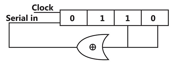
Sign in to UnlockA three bit pseudo random number generator is shown. Initially the value of output is set to 111. The value of output Y after three clock cycles is

Sign in to see the solution
Log in to view the explanation, track your attempts, and keep your progress.
Sign in to UnlockAn SR latch is implemented using TTL gates as shown in the figure. The set and reset pulse inputs are provided using the push-button switches. It is observed that the circuit fails to work as desired. The SR latch can be made functional by changing
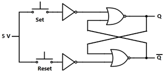
Sign in to see the solution
Log in to view the explanation, track your attempts, and keep your progress.
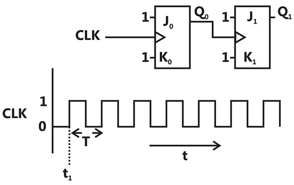
Sign in to UnlockFive JK flip-flops are cascaded to form the circuit shown in Figure. Clock pulses at the frequency of 1MHz are applied as shown. The frequency (in KHz) of the waveform at is __________.

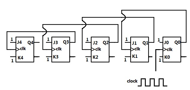
Sign in to see the solution
Log in to view the explanation, track your attempts, and keep your progress.
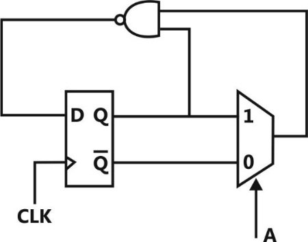
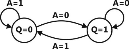
Sign in to UnlockThe digital logic shown in the figure satisfies the given state diagram when Q1 is connected to input A of the XOR gate.
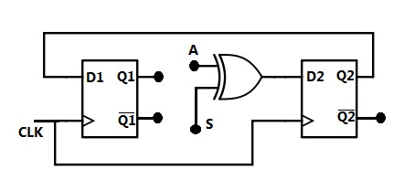
Suppose the XOR gate is replaced by an XNOR gate. Which one of the following options preserves the state diagram?
Input A is connected to

Input A is connected to Q2
Input A is connected to and S is complemented

Input A is connected to
Sign in to see the solution
Log in to view the explanation, track your attempts, and keep your progress.
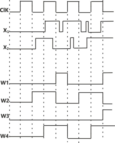
Sign in to UnlockIn the circuit shown, choose the correct timing diagram of the output (y) from the given waveforms W1, W2, W3 and W4.
Sign in to see the solution
Log in to view the explanation, track your attempts, and keep your progress.
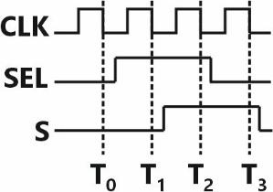
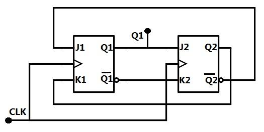
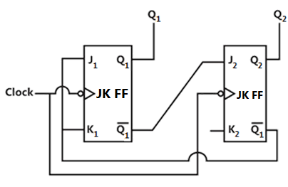
Sign in to UnlockThe outputs of the two flip-flops Q1, Q2 in the figure shown are initialized to 0, 0. The sequence generated at Q1 upon application of clock signal is
Sign in to see the solution
Log in to view the explanation, track your attempts, and keep your progress.
Sign in to UnlockThe circuit shown in the figure is a
Sign in to see the solution
Log in to view the explanation, track your attempts, and keep your progress.
Sign in to UnlockConsider the given circuit. In this circuit, the race around
Sign in to see the solution
Log in to view the explanation, track your attempts, and keep your progress.
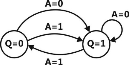
Sign in to UnlockThe state transition diagram for the logic circuit shown is
Sign in to see the solution
Log in to view the explanation, track your attempts, and keep your progress.
Sign in to UnlockAssuming that flip-flops are in reset condition initially, the count sequence observed at in the circuit shown is

Sign in to see the solution
Log in to view the explanation, track your attempts, and keep your progress.
Sign in to UnlockWhen the output Y in the circuit below is “1”, it implies that data has
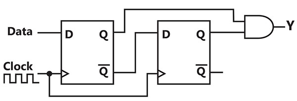
Sign in to see the solution
Log in to view the explanation, track your attempts, and keep your progress.
Sign in to UnlockTwo D flip-flops are connected as a synchronous counter that goes through the following sequence


The connections to the inputs and are


,


,


,

,

Sign in to see the solution
Log in to view the explanation, track your attempts, and keep your progress.
Sign in to UnlockRefer to the NAND and NOR latches shown in the figure. The inputs 1 for both the latches are first made (0, 1) and then, after a few seconds, made (1, 1). The corresponding stable outputs are

Sign in to see the solution
Log in to view the explanation, track your attempts, and keep your progress.
Sign in to UnlockWhat are the counting states for the counter shown in the figure below?
Sign in to see the solution
Log in to view the explanation, track your attempts, and keep your progress.
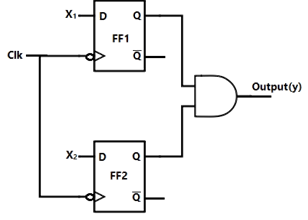
Sign in to UnlockFor each of the positive edge-triggered J-K flip flop used in the following figure, the propagation delay is
Which of the following waveforms correctly represents the output at ?

Sign in to see the solution
Log in to view the explanation, track your attempts, and keep your progress.
Sign in to UnlockFor the circuit shown in the figure, D has a transition from 0 to 1 after CLK changes from 1 to 0. Assume gate delays to be negligible.
Which of the following statements is true?
Sign in to see the solution
Log in to view the explanation, track your attempts, and keep your progress.
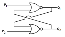
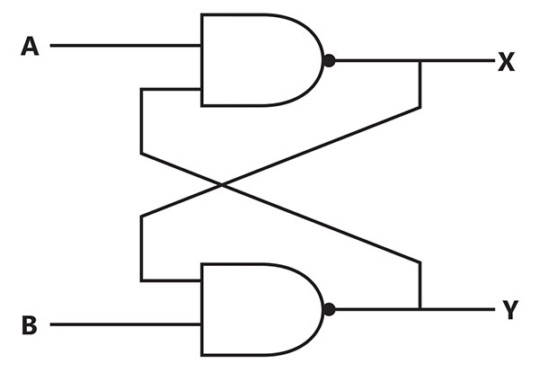
Sign in to UnlockThe following binary values were applied to the X and Y inputs of the NAND latch shown in the figure in the sequence indicated below:
Х= 0, Ү = 1; Х = 0, Ү = 0; Х=1, Ү = 1.
The corresponding stable P, Q outputs will be
Sign in to see the solution
Log in to view the explanation, track your attempts, and keep your progress.
Sign in to UnlockFor the circuit shown, the counter state follows the sequence

Sign in to see the solution
Log in to view the explanation, track your attempts, and keep your progress.
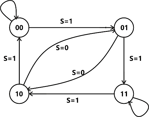
Sign in to UnlockFor the circuit shown in figure below, two 4-bit parallel-in serial-out shift registers loaded with the data shown are used to feed the data to a full adder. Initially, all the flip-flops are in clear state. After applying two clock pulses, the output of the full-adder should be
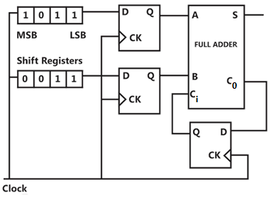
S = 0

S = 0

S = 1
S = 1
Sign in to see the solution
Log in to view the explanation, track your attempts, and keep your progress.
Sign in to UnlockTwo D-flip-flops, as shown below, are to be connected as a synchronous counter that goes through the following sequence


The inputs and respectively should be connected as

and


and

and

and

Sign in to see the solution
Log in to view the explanation, track your attempts, and keep your progress.
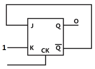
Sign in to UnlockThe present output of an edge triggered JK flip-flop is logic 0. If J=1, then


Sign in to see the solution
Log in to view the explanation, track your attempts, and keep your progress.
Sign in to UnlockFigure shows a ripple counter using positive edge-triggered flip-flops. If the present state of counter is , then its next state will be


Sign in to see the solution
Log in to view the explanation, track your attempts, and keep your progress.
Sign in to UnlockA master slave flip-flop has the characteristic that
Sign in to see the solution
Log in to view the explanation, track your attempts, and keep your progress.
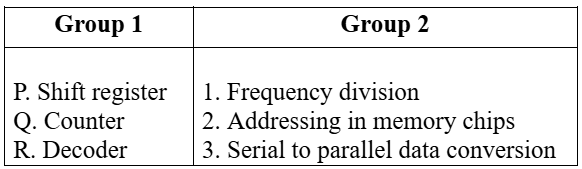
Sign in to UnlockChoose the correct one from among the alternatives A, B, C, D after matching an item from group 1 with the most appropriate item in Group 2.
Sign in to see the solution
Log in to view the explanation, track your attempts, and keep your progress.
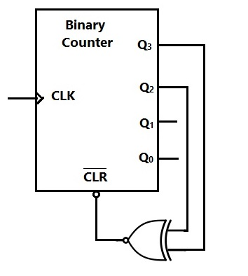
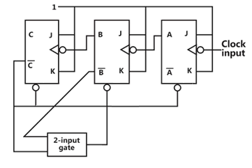
Sign in to UnlockIn the modulo-6 ripple counter shown in Figure, the output of the 2-input gate is used to clear the J-K flip-flops.
The 2-input gate is:
Sign in to see the solution
Log in to view the explanation, track your attempts, and keep your progress.
Sign in to UnlockA 0 to 6 counter consists of 3 flip flops and a combination circuit of 2 input gates(s). The combination circuit consists of
Sign in to see the solution
Log in to view the explanation, track your attempts, and keep your progress.
Sign in to UnlockA 4 bit ripple counter and a 4 bit synchronous counter are made using flip-flops having a propagation delay of 10 ns each. If the worst case delay in the ripple counter and the synchronous counter be R and S respectively, then
Sign in to see the solution
Log in to view the explanation, track your attempts, and keep your progress.
Sign in to UnlockIn the circuit shown in Figure, A is a parallel-in, parallel-out 4-bit register, which loads at the rising edge of the clock C. The input lines are connected to a 4-bit bus, W. Its output acts as the input to a 16×4 ROM whose output is floating when the enable input E is 0. A partial table of contents of the ROM is as follows:
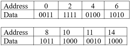
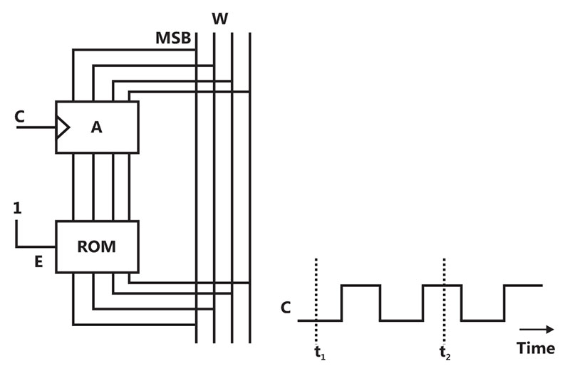
The clock to the register is shown, and the data on the W bus at time is 0110. The data on the bus at time is


Sign in to see the solution
Log in to view the explanation, track your attempts, and keep your progress.
Sign in to UnlockThe circuit in Figure has two CMOS NOR gates, this circuit functions as a:
Sign in to see the solution
Log in to view the explanation, track your attempts, and keep your progress.
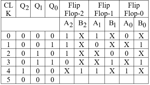
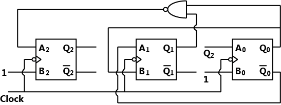
Sign in to UnlockIt is required to design a binary mod-5 synchronous counter using AB flip-flops such that the output changes as ….. and so on. The excitation table for the AB flip-flops is given in table 11.

(a) Write down the state table for the mod-5 counter.
(b) Obtain simplified SOP expressions for the inputs, , , , and in terms of and their complements


(c) Hence, complete the circuit diagram for the mod-5 counter given in figure below using minimum number of 2-input NAND-gate only.
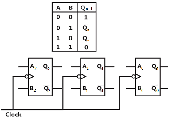
state table for the mod-5 counter


Sign in to see the solution
Log in to view the explanation, track your attempts, and keep your progress.
Sign in to UnlockConsider the following two statements:
Statement 1: Astable multi-vibrator can be used for generating square wave.
Statement 2: Bistable multi-vibrator can be used for storing binary information.
Sign in to see the solution
Log in to view the explanation, track your attempts, and keep your progress.
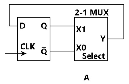
Sign in to UnlockThe digital block in figure is realized using two positive edge triggered D-flip-flops. Assume that for . The circuit in the digital block is given by:


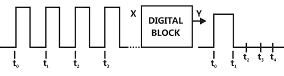
Sign in to see the solution
Log in to view the explanation, track your attempts, and keep your progress.
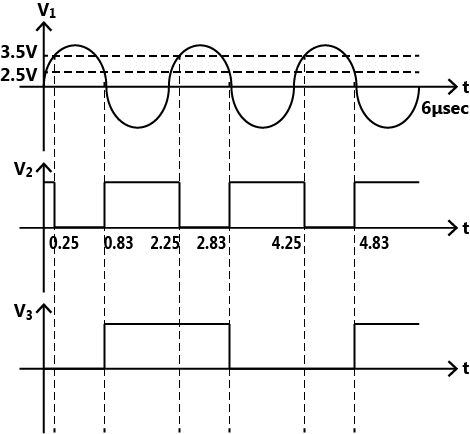
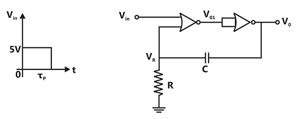
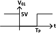
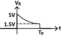
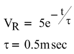
Sign in to UnlockIn Figure, the output of the oscillator, has 10V peak to peak amplitude with zero DC value. The transfer characteristic of the Schmitt inverter is also shown in Figure. Assume that the JK flip-flop is reset at time t = 0.

(a) What is the period and duty cycle of the waveform?

(b) What is the period and duty cycle of the waveform?

(c) Sketch and for the duration. Clearly indicate the exact timings when the waveforms and make a high-to-low and low-to-high transitions.


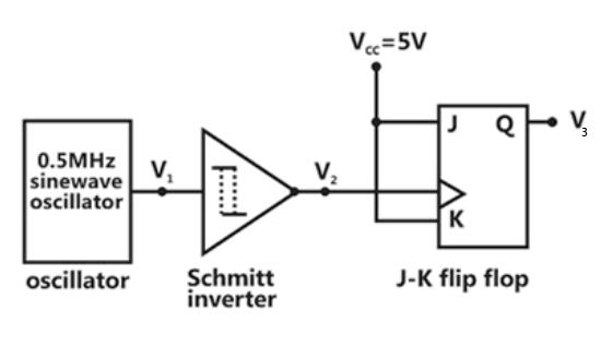
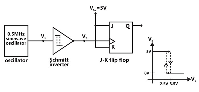
(a) Period of and Duty Cycle = 0.4


(b) Period ofand Duty Cycle = 0.5

(a) Period of and Duty Cycle = 0.5
Sign in to see the solution
Log in to view the explanation, track your attempts, and keep your progress.
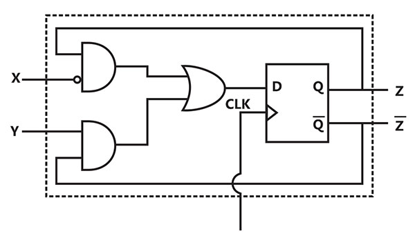
Sign in to UnlockA sequential circuit D flip-flop and logic gates is shown in Figure, where X and Y are the inputs and Z is the output. The circuit is
Sign in to see the solution
Log in to view the explanation, track your attempts, and keep your progress.
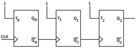
Sign in to UnlockIn Fig.P2.11, the J and K inputs of all the four Flip-Flops are made high. The frequency of the signal at output Y is
Sign in to see the solution
Log in to view the explanation, track your attempts, and keep your progress.
Sign in to UnlockFor the CMOS mono-stable multi-vibrator of figure, , , , and the CMOS NOR gates have a threshold voltage of 1.5 V. is a trigger pulse as shown in the figure.


(a) Plot and as functions of time.


(b) Write the equation for , for .


(c) Find the time period of the output pulse.
(a)
(b)
(c) t=0.6ms
(c) t=0.8ms
Sign in to see the solution
Log in to view the explanation, track your attempts, and keep your progress.
Sign in to UnlockThe ripple counter shown in Figure works as a
Sign in to see the solution
Log in to view the explanation, track your attempts, and keep your progress.
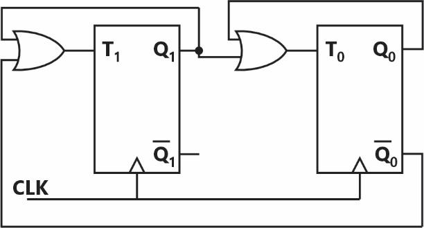
Sign in to UnlockThe circuit diagram of a synchronous counter is shown in Figure. Determine the sequence of states of the counter assuming that the initial state is ‘000’. Give your answer in a tabular form showing the present state, , , J-K inputs and the next state , , . determine the modulus of the counter.


Sign in to see the solution
Log in to view the explanation, track your attempts, and keep your progress.
Sign in to UnlockIn Figure, and , the input B is now replaced by a sequence 101010.... The outputs x and y will be


Fixed at 0 and 1, respectively
. While


. And
Fixed at 1 and 0, respectively
Sign in to see the solution
Log in to view the explanation, track your attempts, and keep your progress.
Sign in to UnlockFigure shows a mod-K counter, here K is equal to
Sign in to see the solution
Log in to view the explanation, track your attempts, and keep your progress.
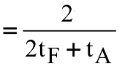
Sign in to UnlockThe mod-5 counter shown in figure counts through states and


(a) Will the counter lockout if it happen to be in any one of the unused states?
(b) Find the maximum rate at which the counter will operate satisfactorily.
Assume the propagation delays of flip-flop and AND gate to be and respectively.


(a) Yes
(a) No
(b) Maximum clock rate

(b) Maximum clock rate
Sign in to see the solution
Log in to view the explanation, track your attempts, and keep your progress.
Sign in to UnlockIn a J-K flip flop we have and . Assuming the flip flop was initially cleared and then clocked for 6 pulses, the sequence at the Q output will be


Sign in to see the solution
Log in to view the explanation, track your attempts, and keep your progress.
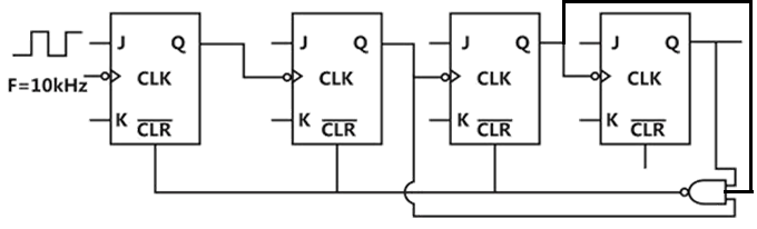
Sign in to UnlockA sequence generator is shown in the figure is the counter status is initialised to 010 using preset/clear inputs.

The clock has a period of 50 ns and transitions take place at the rising clock edge.
Repetition rate of the generated sequence = 8 MHz
Repetition rate of the generated sequence = 4 MHz
Sequence generate at till it repeats 01110
Sequence generate at till it repeats 01010
Sign in to see the solution
Log in to view the explanation, track your attempts, and keep your progress.
Sign in to UnlockA pulse train can be delayed by a finite number of clock periods using
Sign in to see the solution
Log in to view the explanation, track your attempts, and keep your progress.
Sign in to UnlockMatch the following
(a) A shift register can be used
(b) A multiplexer can be used
(c) A decoder can be used
(1) for code conversion
(2) to generate memory chip select
(3) for parallel-to-serial conversion
(4) As a many-to-one switch
(5) For analog-to-digital conversion
Sign in to see the solution
Log in to view the explanation, track your attempts, and keep your progress.
Sign in to UnlockA switch-tail ring counter is made by using a single D flip-flop. The resulting circuit is a
Sign in to see the solution
Log in to view the explanation, track your attempts, and keep your progress.
Sign in to UnlockAn R-S latch is a
Sign in to see the solution
Log in to view the explanation, track your attempts, and keep your progress.
Sign in to UnlockData can be changed from spatial code to temporal code and vice-versa by using
Sign in to see the solution
Log in to view the explanation, track your attempts, and keep your progress.
Sign in to UnlockSynchronous counters are Slower than the ripple counters. ( True=1, False=0)
Sign in to see the solution
Log in to view the explanation, track your attempts, and keep your progress.
Sign in to UnlockA pulse train with a frequency of 1 MHz is counted using a modulo 1024 ripple counter built with J-K flip flops. For proper operation of the counter, the maximum permissible propagation delay per flip flop stage is _______n sec.
Sign in to see the solution
Log in to view the explanation, track your attempts, and keep your progress.
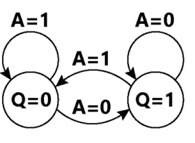
Sign in to UnlockA clocked sequential circuit has three states, A, B and C and one input X. As long as the input X is 0, the circuit alternates between the states A and B. If the input X becomes 1 (either in state A or in State B), the circuit goes to state C and remains in state C as long as long as X continues to be 1. The circuit returns to state A if the input becomes 0 once again and from then on repeats its behaviour. Assume that the state assignments are , and C=10.


Circuit using D flip flops
State table for the circuit
Circuit using D flip flops
State diagram of the circuit
Sign in to see the solution
Log in to view the explanation, track your attempts, and keep your progress.
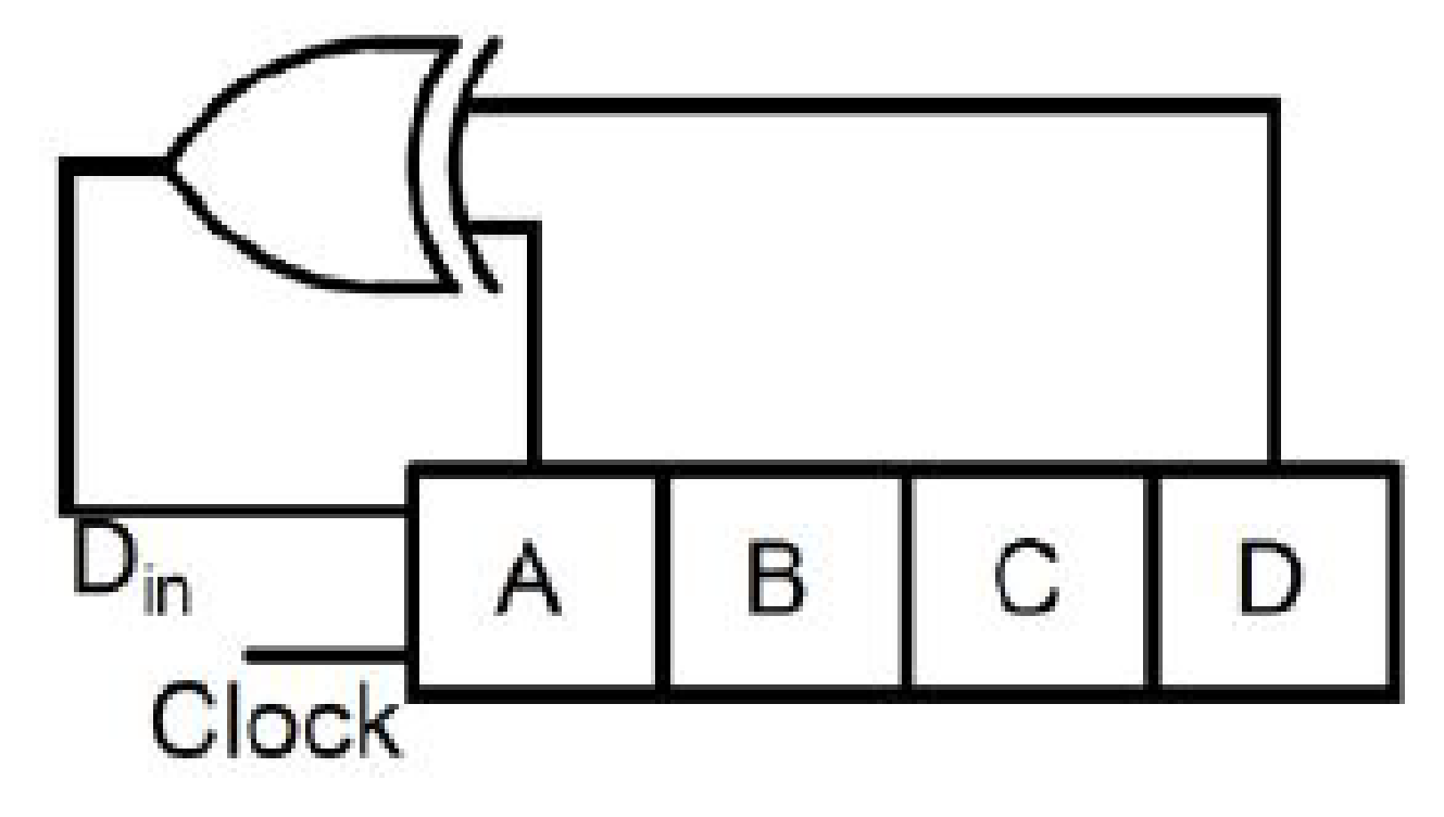
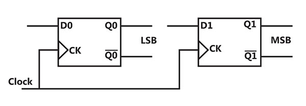
Sign in to UnlockThe initial contents of the 4-bit serial-in-parallel-out, right-shift, shift Register shown in figure, is 0110. After three clock pulses are applied, the contents of the shift Register will be
Sign in to see the solution
Log in to view the explanation, track your attempts, and keep your progress.
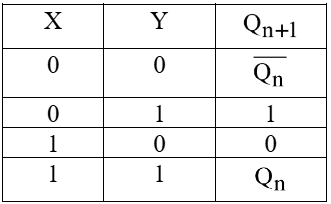
Sign in to UnlockA new clocked X-Y flip-flop is defined with two inputs, X and Y is addition to the clock input. The flip flop functions as follows:
If , the flip flop changes stage with each clock pulse

If , the flip flop state Q becomes 1 with the next clock pulse

If , the flip flop state Q becomes 0 with the next clock pulse

If , no change of state occurs with the clock pulse

It is desired to convert a J-K flip flop into the X-Y flip flop by adding some external gates, if necessary.
Truth table for the X-Y flip flop
Excitation table for the X-Y flip flop
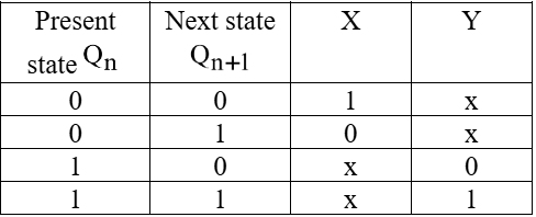
Implement X-Y flip flop using a J-K flip flop.
Implement X-Y flip flop using a J-K flip flop.
Sign in to see the solution
Log in to view the explanation, track your attempts, and keep your progress.
Sign in to UnlockAn S-R FLIP-FLOP can be converted into a T-FLIP-FLOP by connecting S to Q-bar and R to Q.
(True=1, False=0)
Sign in to see the solution
Log in to view the explanation, track your attempts, and keep your progress.
Sign in to Unlock