Analog Electronics
JFET
Practice questions from JFET.
11
Total0
Attempted0
Correct0
IncorrectThe action of a JFET in its equivalent circuit can best be represented as a
Sign in to see the solution
Log in to view the explanation, track your attempts, and keep your progress.
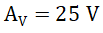
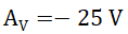
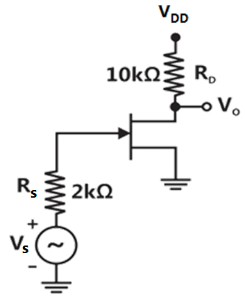
Sign in to UnlockThe voltage gain of the JFET amplifier shown in Figure is

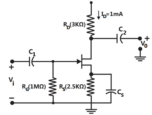

(Assume)

Sign in to see the solution
Log in to view the explanation, track your attempts, and keep your progress.
Sign in to UnlockAn n-channel JEFT has and. Its trans-conductance (in milliohm) for an applied gate-to-source voltage of -2V is


Sign in to see the solution
Log in to view the explanation, track your attempts, and keep your progress.
Sign in to UnlockA JFET having and is used in a common-source configuration as shown in Figure. The JEFT capacitances are , and . Determine the ac small signal mid-band voltage gain and the upper -3dB frequency of the circuit.


The upper -3dB frequency = 1.39 MHz
The upper -3dB frequency = 2.39 MHz
Sign in to see the solution
Log in to view the explanation, track your attempts, and keep your progress.
Sign in to UnlockTwo identical FETs, each characterized by the parameters and are connected in parallel. The composite FET is then characterized by the parameters

and


and

and

and
Sign in to see the solution
Log in to view the explanation, track your attempts, and keep your progress.
Sign in to UnlockThe JFET in the circuit of Figure, is characterized by the parameters and.

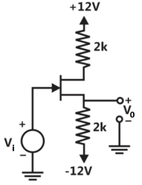
Find
(a) if


(b) if


Sign in to see the solution
Log in to view the explanation, track your attempts, and keep your progress.
Sign in to UnlockAn n-channel JEFT has and . Its maximum transconductance is __________mS.


Sign in to see the solution
Log in to view the explanation, track your attempts, and keep your progress.
Sign in to UnlockMatch the following
In a JEFT if
(A) The pinch-off voltage decreases
(B) The trans-conductance increases
(C) The transit time of the carriers in the channel is reduced
(1) The channel doping is reduced
(2) The channel length is increased
(3) The conductivity of channel is increased
(4) The channel length is reduced
(5) The Gate area is reduced
Sign in to see the solution
Log in to view the explanation, track your attempts, and keep your progress.
Sign in to UnlockThe transit time of the current carriers through the channel of an FET decides its switching characteristic. ( True=1, False=0)
Sign in to see the solution
Log in to view the explanation, track your attempts, and keep your progress.
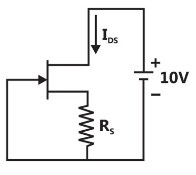
Sign in to UnlockThe JFET in the circuit shown in figure has an and . The value of the resistance for a drain current is (select the nearest value)


Sign in to see the solution
Log in to view the explanation, track your attempts, and keep your progress.
Sign in to UnlockA JFET with the following parameters is used in a single stage common source amplifier with a load resistance of . Calculate the high frequency cut off (upper 3 dB cut off frequency in Mhz) of the amplifier.


Sign in to see the solution
Log in to view the explanation, track your attempts, and keep your progress.
Sign in to Unlock