Analog Electronics
MOSFET
Practice questions from MOSFET.
63
Total0
Attempted0
Correct0
IncorrectWhich of the following statements is/are TRUE with respect to ideal MOSFET based DC-coupled single-stage amplifiers having finite load resistors?
Sign in to see the solution
Log in to view the explanation, track your attempts, and keep your progress.
Sign in to UnlockIn the circuit below, assume that the long channel NMOS transistor is biased in saturation. The small signal trans-conductance of the transistor is . Neglect body effect, channel length modulation and intrinsic device capacitances. The small signal input impedance is________.


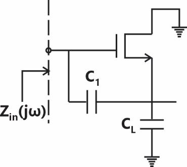




Sign in to see the solution
Log in to view the explanation, track your attempts, and keep your progress.
Sign in to UnlockFor the closed loop amplifier circuit shown below, the magnitude of open loop low frequency small signal voltage gain is 40. All the transistors are biased in saturation. The current source is ideal. Neglect body effect, channel length modulation and intrinsic device capacitances. The closed loop low frequency small signal voltage gain (rounded off to three decimal places) is________.


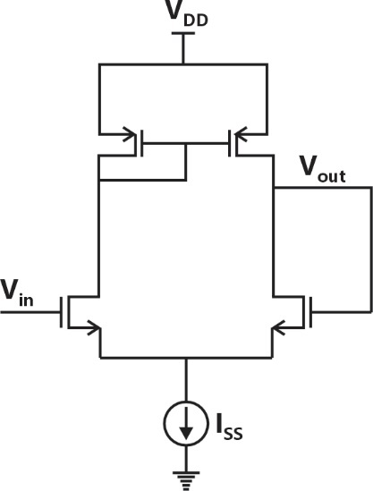
Sign in to see the solution
Log in to view the explanation, track your attempts, and keep your progress.
Sign in to UnlockIn the circuit shown below, the transistors and are biased in saturation. Their small signal transconductances are and respectively. Neglect body effect, channel length modulation and intrinsic device capacitances.




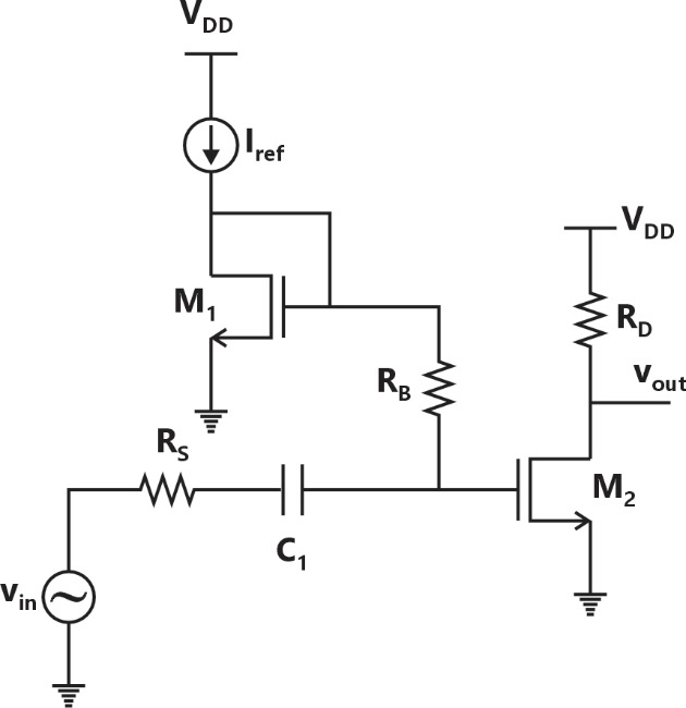




Sign in to see the solution
Log in to view the explanation, track your attempts, and keep your progress.
Sign in to UnlockConsider a MOS capacitor made with p-type silicon. It has an oxide thickness of , a fixed positive oxide charge of at the oxide-silicon interface, and a metal work function of . Assume that the relative permittivity of the oxide is 4 and the absolute permittivity of free space is . If the flatband voltage is , the work function of the -type silicon (in , rounded off to two decimal places) is________.







Sign in to see the solution
Log in to view the explanation, track your attempts, and keep your progress.
Sign in to UnlockAn NMOS transistor operating in the linear region has of at of 0.1 V. Keeping constant, the is increased to 1.5 V.




Given that , the

transconductance at the new operating point
(in , rounded off to two decimal places) is________.

Sign in to see the solution
Log in to view the explanation, track your attempts, and keep your progress.
Sign in to UnlockFor a MOS capacitor, and are the flat-band voltage and the threshold voltage, respectively. The variation of the depletion width for varying gate voltage is best represented by




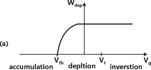
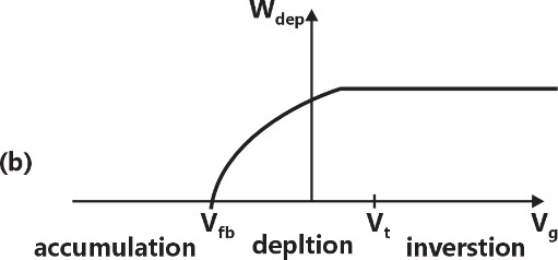
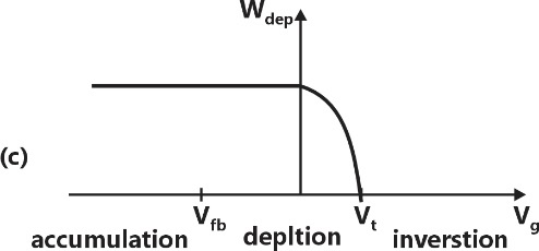
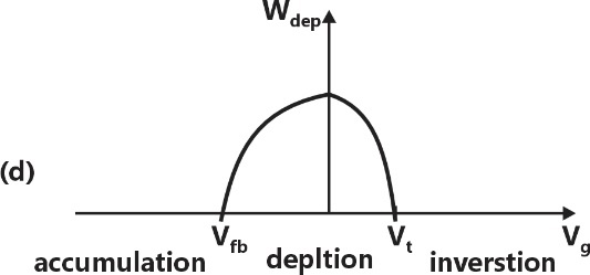
Sign in to see the solution
Log in to view the explanation, track your attempts, and keep your progress.
Sign in to UnlockIn the circuit shown below, and are bias voltages. Based on input and output impedances, the circuit behaves as a


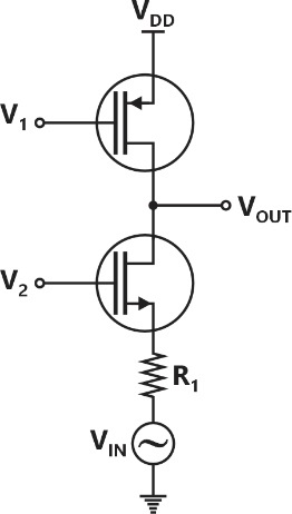
Sign in to see the solution
Log in to view the explanation, track your attempts, and keep your progress.
Sign in to UnlockA cascade of common-source amplifiers in a unity gain feedback configuration oscillates when
the closed loop gain is less than 1 and the phase shift is less than .

the closed loop gain is greater than 1 and the phase shift is less than .
the closed loop gain is less than 1 and the phase shift is greater than .
the closed loop gain is greater than 1 and the phase shift is greater than .
Sign in to see the solution
Log in to view the explanation, track your attempts, and keep your progress.
Sign in to UnlockIn the circuit below, the voltage is _______V. (rounded off to two decimal places)

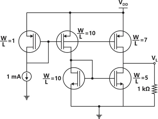
Sign in to see the solution
Log in to view the explanation, track your attempts, and keep your progress.
Sign in to UnlockConsider the CMOS circuit shown in the figure (substrates are connected to their respective sources). The gate width ( ) to gate length ratios of the transistors are as shown. Both the transistors have the same gate oxide capacitance per unit area. For the pMOSFET, the threshold voltage is and the mobility of holes is and the mobility of electrons is . The steady state output voltage is ________.







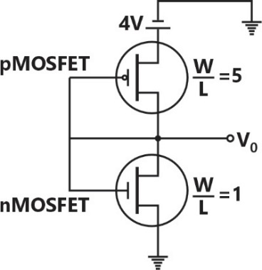
Sign in to see the solution
Log in to view the explanation, track your attempts, and keep your progress.
Sign in to UnlockThe ideal long channel nMOSFET and pMOSFET devices shown in the circuits have threshold voltages of and , respectively. The MOSFET substrates are connected to their respective sources. Ignore leakage currents and assume that the capacitors are initially discharged. For the applied voltages as shown, the steady state voltages are ________.
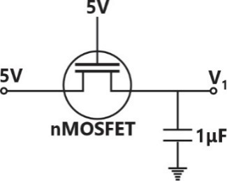
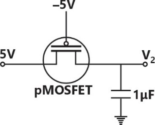




Sign in to see the solution
Log in to view the explanation, track your attempts, and keep your progress.
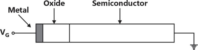
Sign in to UnlockAn ideal MOS capacitor ( -type semiconductor) is shown in the figure. The MOS capacitor is under strong inversion with . The corresponding inversion charge density is . Assume oxide capacitance per unit area as . For , the value of is __________ (rounded off to one decimal place).








Sign in to see the solution
Log in to view the explanation, track your attempts, and keep your progress.
Sign in to UnlockConsider an ideal long channel nMOSFET (enhancement-mode) with gate length and width . The product of electron mobility and oxide capacitance per unit area is . The threshold voltage of the transistor is 1V. For a gate-to-source voltage and drain-to source voltage (substrate connected to the source), the maximum value of the drain-to-source current is__________.











Sign in to see the solution
Log in to view the explanation, track your attempts, and keep your progress.
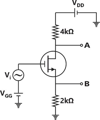
Sign in to UnlockConsider the circuit shown with an ideal long channel nMOSFET (enhancement mode, substrate is connected to the source). The transistor is appropriately biased in the saturation region with and such that it acts as a linear amplifier. is the small-signal ac input voltage. and represent the small-signal voltages at the nodes A and B, respectively. The value of is ________ (rounded off to one decimal place).






Sign in to see the solution
Log in to view the explanation, track your attempts, and keep your progress.
Sign in to UnlockIn the circuit shown in the figure, the transistors and are operating in saturation. The channel length modulation coefficients of both the transistors are non-zero. The transconductance of the MOSFETs and are and respectively, and the internal resistance of the MOSFETs and are and , respectively.






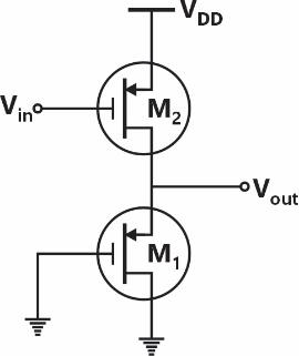
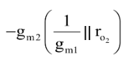
Ignoring the body effect, the AC small signal voltage gain of the circuit is



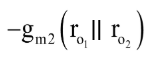
Sign in to see the solution
Log in to view the explanation, track your attempts, and keep your progress.
Sign in to UnlockFor an n-channel silicon MOSFET with gate oxide thickness, the substrate sensitivity is found to be at a substrate voltage , where is the threshold voltage of the MOSFET. Assume that, , where is the separation between the Fermi energy level and the intrinsic level in the bulk. Parameters given are





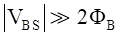



Electron charge

Vacuum permittivity

Relative permittivity of silicon

Relative permittivity of oxide

The doping concentration of the substrate is




Sign in to see the solution
Log in to view the explanation, track your attempts, and keep your progress.
Sign in to UnlockFor the transistor in the circuit shown in the figure, and , where is the mobility of electron, is the oxide capacitance per unit area, is the width and is the length.





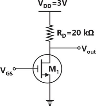
The channel length modulation coefficient is ignored. If the gate-to-source voltage is to keep the transistor at the edge of saturation, then the threshold voltage of the transistor (rounded off to one decimal place) is _______ V.

Sign in to see the solution
Log in to view the explanation, track your attempts, and keep your progress.
Sign in to Unlockhe band diagram of a -type semiconductor with a band-gap of is shown. Using this semiconductor, a MOS capacitor having of of and a metal work function of is fabricated. There is no charge within the oxide. If the voltage across the capacitor is . the magnitude of depletion charge per unit area (in ) is







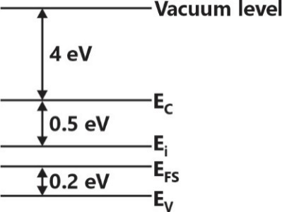




Sign in to see the solution
Log in to view the explanation, track your attempts, and keep your progress.
Sign in to UnlockAn enhancement MOSFET of threshold voltage 3 is being used in the sample and hold circuit given below. Assume that the substrate of the MOS device is connected to . If the input voltage lies between . the minimum and the maximum values of required for proper sampling and holding respectively, are





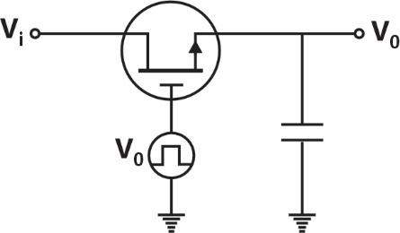
and


and


and

and


Sign in to see the solution
Log in to view the explanation, track your attempts, and keep your progress.
Sign in to UnlockUsing the incremental low frequency small-signal model of the MOS device, the Norton equivalent resistance of the following circuit is
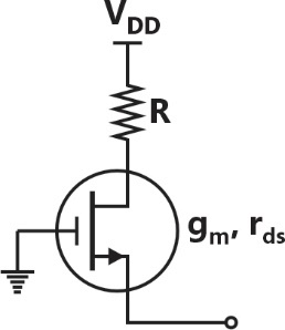




Sign in to see the solution
Log in to view the explanation, track your attempts, and keep your progress.
Sign in to UnlockIn the circuit shown,and. The other relevant parameters are mentioned in the figure. Ignoring the effect of channel length modulation and the body effect, the value ofis ______mA [Rounded off to 1 decimal place]



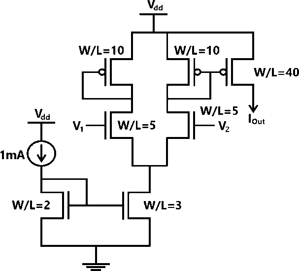
Sign in to see the solution
Log in to view the explanation, track your attempts, and keep your progress.
Sign in to UnlockIn the circuit shown, the threshold voltages of the pMOSand nMOStransistor are both equal to 1V. All the transistor have the same output resistance of 6MΩ. The other parameter are listed below:





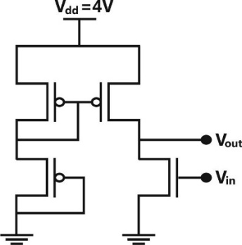
andare the carrier mobilities andis the capacitance per unit area. Ignoring the effect of channel length modulation and body bias, the gain of the circuit is _______ (rounded off to 1 decimal place)



Sign in to see the solution
Log in to view the explanation, track your attempts, and keep your progress.
Sign in to UnlockConsider a long channel MOSFET with a channel length 1µm and width 10µm. The device parameters are acceptor concentration; electron mobility, oxide capacitance/area , threshold voltage. The rain saturation currentfor a gate voltage of 5V is ______ mA [rounded off to two decimal places]






Sign in to see the solution
Log in to view the explanation, track your attempts, and keep your progress.
Sign in to UnlockIn the circuits shown, the threshold voltage of each nMOS transistor is 0.6 V. Ignoring the effect of channel length modulation and body bias, the values of Vout1 and Vout2. Respectively, in volts, are
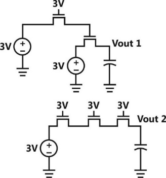
Sign in to see the solution
Log in to view the explanation, track your attempts, and keep your progress.
Sign in to UnlockCMOS inverter, designed to have a mid-point voltage equal to half of as shown in the figure, has the following parameters:





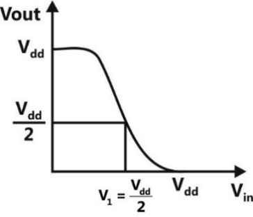
The ratio of is equal to ___________ (rounded off to 3 decimal places).

Sign in to see the solution
Log in to view the explanation, track your attempts, and keep your progress.
Sign in to UnlockTwo identical. nMOS transistors and are connected as shown below. The circuit is used as an amplifier with the input connected between G and S terminals and the output taken between D and S terminals, , and are so adjusted that both transistors are in saturation. The transconductance of this combination is defined as while the output resistance is , where is the current flowing into the drain of . Let,, be the transconductances and , be the output resistances of transistors and , respectively.











Which of the following statements about estimates for and is correct?


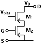
and


and

and


and

Sign in to see the solution
Log in to view the explanation, track your attempts, and keep your progress.
Sign in to UnlockIn the circuit shown below, the (W/L) value for is twice that for. The two NMOS transistors are otherwise identical. The threshold voltage for both transistors is 1.10V. Note thatfor must be >1.0 V. Current through the NMOS transistors can be modelled as


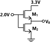

For


For

The voltage (in volts, accurate to two decimal places) atis ________

Sign in to see the solution
Log in to view the explanation, track your attempts, and keep your progress.
Sign in to UnlockAssuming that transistors are identical and have a threshold voltage of 1 V, the state of transistors are respectively

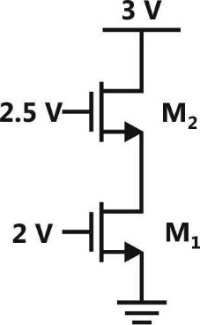
Sign in to see the solution
Log in to view the explanation, track your attempts, and keep your progress.
Sign in to UnlockIn the circuit shown in the figure, the channel length modulation of all transistors is non-zero (λ≠0). Also, all transistors operate in saturation and have negligible body effect. The ac small signal voltage gain of the circuit is

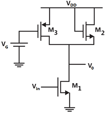




Sign in to see the solution
Log in to view the explanation, track your attempts, and keep your progress.
Sign in to UnlockIn the circuit shown in the figure, transistor is in saturation and has transconductance Siemens. Ignoring internal parasitic capacitances and assuming the channel length modulation λ to be zero, the small signal input pole frequency (in kHz) is ______.

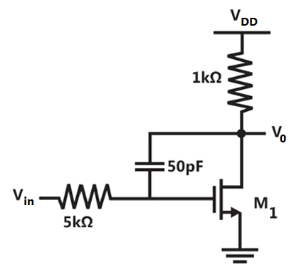
Sign in to see the solution
Log in to view the explanation, track your attempts, and keep your progress.
Sign in to UnlockFor the NMOSFET in the circuit shown, the threshold voltage is , where . The source voltage is varied from 0 to . Neglecting the channel length modulation, the drain current as a function of is represented by





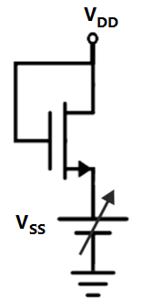
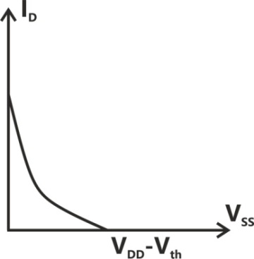
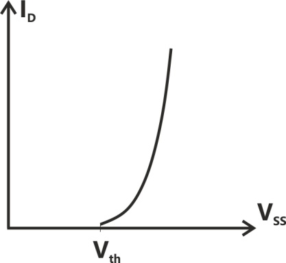
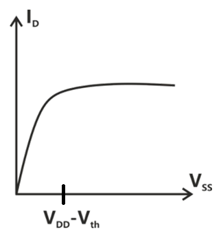
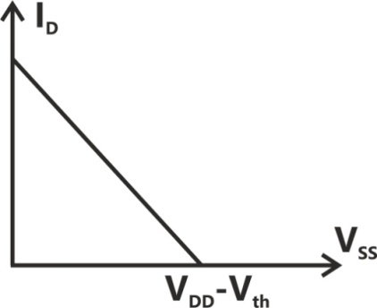
Sign in to see the solution
Log in to view the explanation, track your attempts, and keep your progress.
Sign in to UnlockIn the circuit shown, both the enhancement mode NMOS transistors have the following characteristics: , Assume that the channel length modulation parameter λ is zero and body is shorted to source. The minimum supply voltage (in volts) needed to ensure that transistor operates in saturation mode of operation is _______.


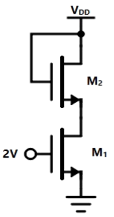
Sign in to see the solution
Log in to view the explanation, track your attempts, and keep your progress.
Sign in to UnlockIn the following circuit employing pass transistor logic, all NMOS transistors are identical with a threshold voltage 1V. Ignoring the body-effect, the output voltages at P, Q and R are,
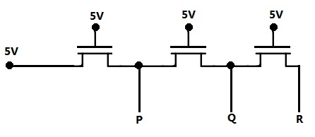
Sign in to see the solution
Log in to view the explanation, track your attempts, and keep your progress.
Sign in to UnlockA depletion type N-channel MOSFET is biased in its linear region for use as a voltage controlled resistor. Assume threshold voltage, , , W/L = 100, and . The value of the resistance of the voltage controlled resistor (in Ω) is __________.





Sign in to see the solution
Log in to view the explanation, track your attempts, and keep your progress.
Sign in to UnlockFor the n-channel MOS transistor shown in the figure, the threshold voltage is 0.8 V. Neglect channel length modulation effects. When the drain
voltage , the drain current was found to be 0.5mA. If is adjusted to be 2 V by changing the values of R and , the new value of (in mA) is



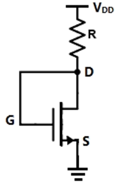
Sign in to see the solution
Log in to view the explanation, track your attempts, and keep your progress.
Sign in to UnlockFor the MOSFETs shown in the figure, the threshold voltage and . The value of (in mA) is _______.


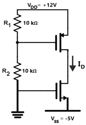
Sign in to see the solution
Log in to view the explanation, track your attempts, and keep your progress.
Sign in to UnlockFor the MOSFET shown in the figure, assume W/L = 2, , and . The transistor switches from saturation region to linear region when (in Volts) is__________.




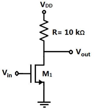
Sign in to see the solution
Log in to view the explanation, track your attempts, and keep your progress.
Sign in to UnlockIn a MOSFET operating in the saturation region, the channel length modulation effect causes
Sign in to see the solution
Log in to view the explanation, track your attempts, and keep your progress.
Sign in to UnlockThe small-signal resistance in offered by the n-channel MOSFET M shown in the figure below, at a bias point of is (device data for M: device trans-conductance parameter, threshold voltage , and neglect body effect and channel length modulation effects)





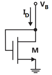
Sign in to see the solution
Log in to view the explanation, track your attempts, and keep your progress.
Sign in to UnlockThe ac schematic of an NMOS common-source stage is shown in the figure below, where part of the biasing circuits has been omitted for simplicity. For the n-channel MOSFET M, the trans-conductance, and body effect and channel length modulation effect are to be neglected. The lower cut-off frequency in Hz of the circuit is approximately at

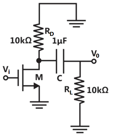
Sign in to see the solution
Log in to view the explanation, track your attempts, and keep your progress.
Sign in to UnlockIn the CMOS circuit shown, electron and hole mobilities are equal, and and are equally sized. The device is in the linear region if
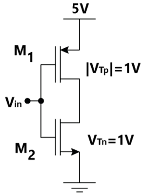




Sign in to see the solution
Log in to view the explanation, track your attempts, and keep your progress.
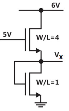
Sign in to UnlockIn the circuit shown below, for the MOS transistors, and the threshold voltage.The voltage at the source of the upper transistor is



Sign in to see the solution
Log in to view the explanation, track your attempts, and keep your progress.
Sign in to UnlockConsider the CMOS circuit shown,
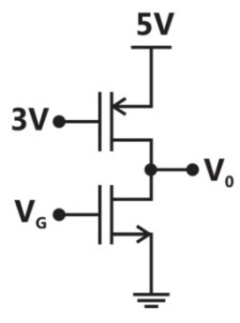
Where the gate voltage of the n-MOSFET is increased from zero, while the gate voltage of the p-MOSFET is kept constant at 3 V. Assume that, for both transistors, the magnitude of the threshold voltage is 1 V and the product of the trans-conductance parameter and the (W/L), is.


For small increase in beyond 1 V, which of the following gives the correct description of the region of operation of each MOSFET?
Sign in to see the solution
Log in to view the explanation, track your attempts, and keep your progress.
Sign in to UnlockConsider the CMOS circuit shown,
Where the gate voltage of the n-MOSFET is increased from zero, while the gate voltage of the p-MOSFET is kept constant at 3 V. Assume that, for both transistors, the magnitude of the threshold voltage is 1 V and the product of the trans-conductance parameter and the (W/L), is.
Estimate the output voltage for .


[Hint: Use the approximate current-voltage equation for each MOSFET,]




Sign in to see the solution
Log in to view the explanation, track your attempts, and keep your progress.
Sign in to UnlockThe drain current of a MOSFET in saturation is given by where K is a constant. The magnitude of the trans-conductance is






Sign in to see the solution
Log in to view the explanation, track your attempts, and keep your progress.
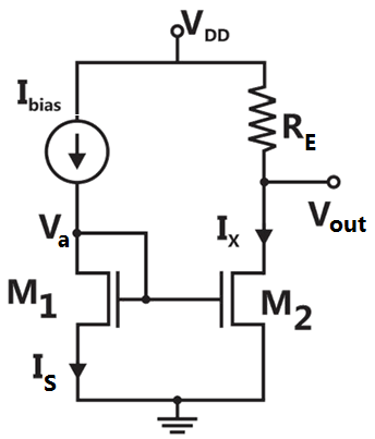
Sign in to UnlockFor the circuit shown in the following figure, transistors and are identical NMOS transistors. Assumes that is in saturation and the output is unloaded. The current is related to as






Sign in to see the solution
Log in to view the explanation, track your attempts, and keep your progress.
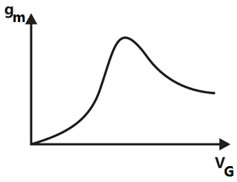
Sign in to UnlockThe measured trans-conductance of an NMOS transistor operating in the linear region is plotted against the gate voltage at a constant drain voltage. Which of the following figures represents the expected dependence of on ?

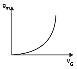
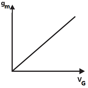
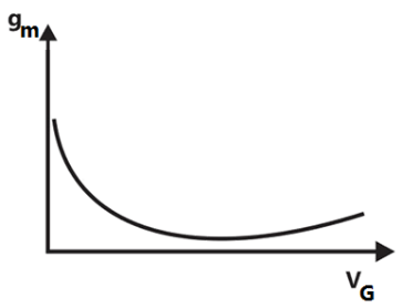
Sign in to see the solution
Log in to view the explanation, track your attempts, and keep your progress.
Sign in to UnlockTwo identical NMOS transistors and are connected as shown below. is chosen so that both transistors are in saturation. The equivalent of the pair is defined to be at constant. The equivalent of the pair is



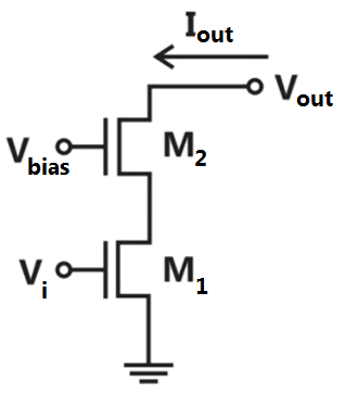
The sum of individual of the transistors

The product of individual of the transistors
Nearly equal to the of M1
Nearly equal to of M2

Sign in to see the solution
Log in to view the explanation, track your attempts, and keep your progress.
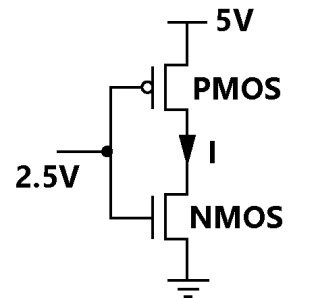
Sign in to UnlockIn the CMOS inverter circuit shown, if the trans-conductance parameters of the NMOS and PMOS transistors are and their threshold voltages are, the current I is


Sign in to see the solution
Log in to view the explanation, track your attempts, and keep your progress.
Sign in to UnlockAn n-channel depletion MOSFET has following two points on its curve:

(i) at and


(ii) Volts at


Which of the following Q-points will give the highest trans-conductance gain for small signals?
Volts
Volts

Volts
Volts

Sign in to see the solution
Log in to view the explanation, track your attempts, and keep your progress.
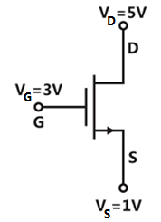
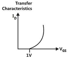
Sign in to UnlockFor an n-channel MOSFET and its transfer curve shown in figure, the threshold voltage is
Sign in to see the solution
Log in to view the explanation, track your attempts, and keep your progress.
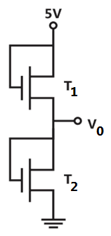
Sign in to UnlockBoth transistors and in figure have a threshold voltage of 1 Volt. The device parameters and of and are, respectively, and. The output voltage is







Sign in to see the solution
Log in to view the explanation, track your attempts, and keep your progress.
Sign in to Unlock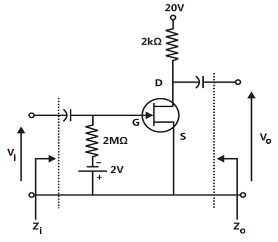
Given, ,



and of the circuit are respectively


and


and

Infinity and
Infinity and
Sign in to see the solution
Log in to view the explanation, track your attempts, and keep your progress.
Sign in to UnlockGiven, ,
and under DC conditions are respectively


Sign in to see the solution
Log in to view the explanation, track your attempts, and keep your progress.
Sign in to UnlockGiven, ,
Trans-conductance in milli-Siemens (mS) and voltage gain of the amplifier are respectively
Sign in to see the solution
Log in to view the explanation, track your attempts, and keep your progress.
Sign in to UnlockMOSFET can be used as a
Sign in to see the solution
Log in to view the explanation, track your attempts, and keep your progress.
Sign in to UnlockThe effective channel length of a MOSFET in saturation decreases with increase in
Sign in to see the solution
Log in to view the explanation, track your attempts, and keep your progress.
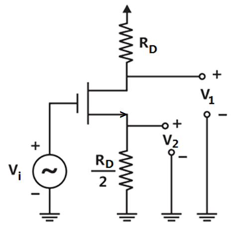
Sign in to UnlockIn the MOSFET amplifier of Figure, the signal outputs andobeys the relationship






Sign in to see the solution
Log in to view the explanation, track your attempts, and keep your progress.
Sign in to UnlockCircuit shown in the figure is an NMOS shift register. All transistors are NMOS enhancement type with threshold voltage. Supply used is


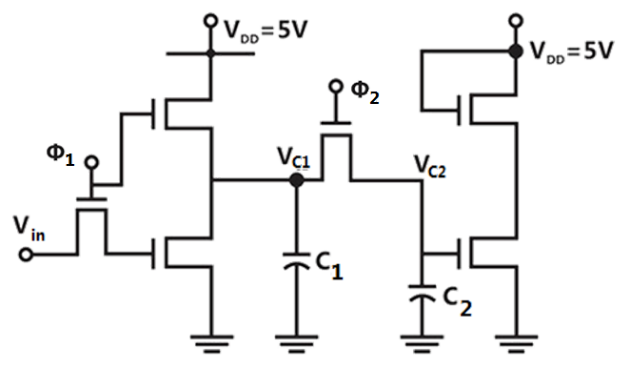
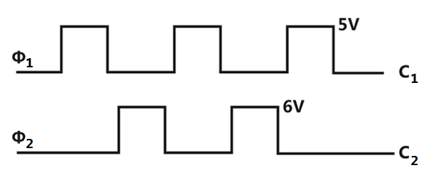
Two non-overlapping clock and are as shown in the figure is and have large pulse widths.


All capacitors are initially discharged and the input volt is applied. If values of capacitors are and , find out voltage on capacitor after goes low. Neglect body-effect on in your evaluation






Sign in to see the solution
Log in to view the explanation, track your attempts, and keep your progress.
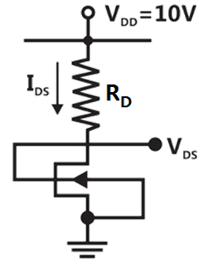
Sign in to UnlockGiven an NMOS circuit as shown in the figure is the specifications of the circuit are; and . Evaluate and for the circuit. Neglect body –effect for




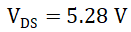
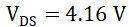
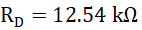
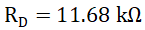
Sign in to see the solution
Log in to view the explanation, track your attempts, and keep your progress.
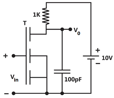
Sign in to UnlockAn n-channel MOSFET (T) having a of 2V [Threshold voltage] is used in the circuit shown in figure.
Initially, t is off an in steady state. At time, a step voltage of magnitude 4V is applied to the input so that the MOSFET turns ‘ON’ instantaneously. Calculate the time taken (ns) for the output to fall to 5V. The device constant of the MOSFET, , ,





Sign in to see the solution
Log in to view the explanation, track your attempts, and keep your progress.
Sign in to UnlockIn figure, the n-channel MOSFETs are identical and their current voltage characteristics are given by the following expressions:
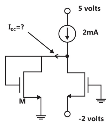
For

For

Where and are the gate source and drain source voltages respectively and is the drain current. The current flowing through the transistor ‘M’ is equal to _______mA




Sign in to see the solution
Log in to view the explanation, track your attempts, and keep your progress.
Sign in to Unlock