Electronic Devices
MOSFET - EDC
Practice questions from MOSFET - EDC.
46
Total0
Attempted0
Correct0
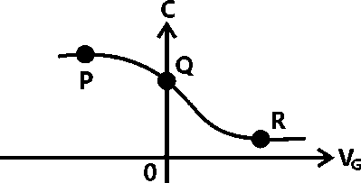
IncorrectThe figure is the high frequency C-V curve of a MOS capacitor (at T=300 K) with and no oxide charges. The flat-band inversion and accumulation conditions are represented respectively by the points

Sign in to see the solution
Log in to view the explanation, track your attempts, and keep your progress.
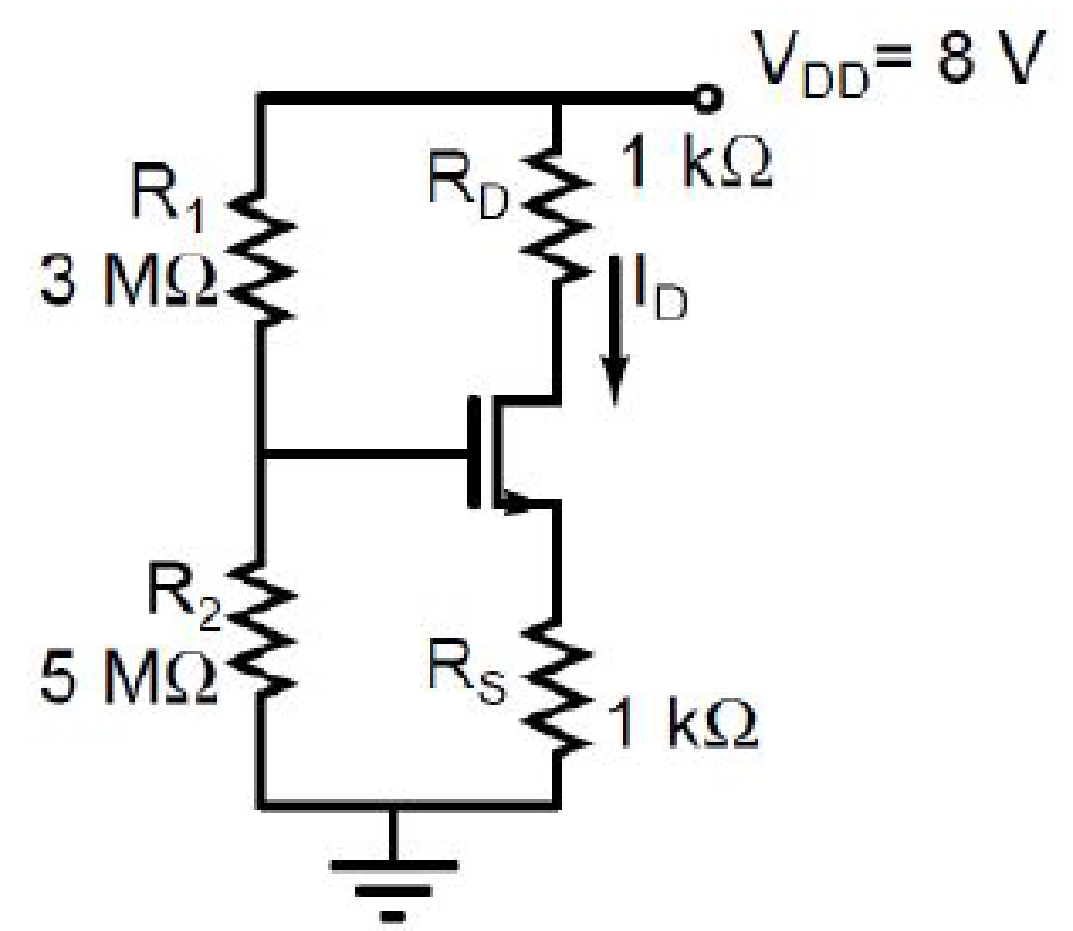
Sign in to UnlockFor the circuit shown, assume that the NMOS transistor is in saturation. Its threshold voltage and its trans-conductance parameter . Neglect channel length modulation and body bias effects. Under these conditions, the drain current in mA is ________ .



Sign in to see the solution
Log in to view the explanation, track your attempts, and keep your progress.
Sign in to UnlockAn n-channel enhancement mode MOSFET is biased at , where is the gate-to-source voltage, is the drain-to-source voltage and is the threshold voltage. Considering channel length modulation effect to be significant, the MOSFET behaves as a




Sign in to see the solution
Log in to view the explanation, track your attempts, and keep your progress.
Sign in to UnlockConsider an n-channel MOSFET having width W, length L, electron mobility in the channel and oxide capacitance per unit area . If gate-to-source voltage , drain-to-source voltage , threshold voltage , then the trans conductance (in mA/V) is _____







Sign in to see the solution
Log in to view the explanation, track your attempts, and keep your progress.
Sign in to UnlockA MOS capacitor is fabricated on p-type Si (Silicon) where the metal work function is 4.1 and electron affinity of Si is 4.0 eV. where and are the conduction band minimum and the Fermi energy levels of Si, respectively. Oxide , oxide thickness and electronic charge C. If the measured flat band voltage of this capacitor is – 1V, then the magnitude of the fixed charge at the oxide-semiconductor interface, in , is ___________








Sign in to see the solution
Log in to view the explanation, track your attempts, and keep your progress.
Sign in to UnlockTwo n-channel MOSFETs, and , are identical in all respects except that the width of is double that of . Both the transistors are biased in the saturation region of operation, but the gate overdrive voltage of is double that of , where are the gate-to-source voltage and threshold voltage of the transistors, respectively. If the drain current and trans conductance of are respectively, the corresponding values of these two parameters for T2 are









Sign in to see the solution
Log in to view the explanation, track your attempts, and keep your progress.
Sign in to UnlockConsider the following statements for a metal oxide semiconductor field effect transistor (MOSFET).
P: As channel length reduces, OFF-state current increases.
Q: As channel length reduces, output resistance increases.
R. As channel length reduces, threshold voltage remains constant.
S: As channel length reduces, ON current increases.
Which of the above Statements are INCORRECT?
Sign in to see the solution
Log in to view the explanation, track your attempts, and keep your progress.
Sign in to UnlockConsider an n-channel metal oxide semiconductor field effect transistor (MOSFET) with a gate-to source
voltage of 1.8 V. Assume that, , the threshold voltage is0.3V, and the channel length modulation parameter is 0.09 . In the saturation region, the drain conductance (in micro Siemens) is_____________



Sign in to see the solution
Log in to view the explanation, track your attempts, and keep your progress.
Sign in to UnlockA long-channel NMOS transistor is biased in the linear region with mV and is used as a resistance. Which one of the following statements is NOT correct?

If the device width W is increased, the resistance decreases.
If the threshold voltage is reduced, the resistance decreases.
If the device length L is increased, the resistance increases.
Ifis increased, the resistance increases.
Sign in to see the solution
Log in to view the explanation, track your attempts, and keep your progress.
Sign in to UnlockA voltage is applied across a MOS capacitor with metal gate and p-type silicon substrate at. The inversion carrier density (in number of carriers per unit area) for is . For , the inversion carrier density is . What is the value of the inversion carrier density for?










Sign in to see the solution
Log in to view the explanation, track your attempts, and keep your progress.
Sign in to UnlockConsider a long-channel NMOS transistor with source and body connected together. Assume that the electron mobility is independent of and . Given,
for and ,



for and ,


Where and


The threshold voltage (in volts) of the transistor is ________.
Sign in to see the solution
Log in to view the explanation, track your attempts, and keep your progress.
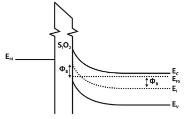
Sign in to UnlockThe figure shows the band diagram of a Metal Oxide Semiconductor (MOS). The surface region of this MOS is in
Sign in to see the solution
Log in to view the explanation, track your attempts, and keep your progress.
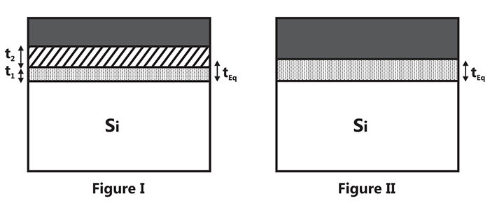
Sign in to UnlockFigures I and II show two MOS capacitors of unit area. The capacitor in figure I has insulator materials X (of thickness =1 nm and dielectric constant = 4) and Y (of =3 nm and dielectric constant = 20). The capacitor in figure II has only insulator material X of thickness If the capacitors are of equal capacitance, then the value of (in nm) is __________





Sign in to see the solution
Log in to view the explanation, track your attempts, and keep your progress.
Sign in to UnlockA MOSFET in saturation has a drain current of 1 mA for = 0.5 V. If the channel length modulation coefficient is 0.05 , the output resistance (in kΩ) of the MOSFET is _________.
Sign in to see the solution
Log in to view the explanation, track your attempts, and keep your progress.
Sign in to UnlockIn a MOS capacitor with an oxide layer thickness of 10 nm, the maximum depletion layer thickness is 100 nm. The permittivities of the semiconductor and the oxide layer are and respectively. Assuming , the ratio of the maximum capacitance to the minimum capacitance of this MOS capacitor is ________.



Sign in to see the solution
Log in to view the explanation, track your attempts, and keep your progress.
Sign in to UnlockThe current in an enhancement mode NMOS transistor biased in saturation mode was measured to be 1mA at a drain-source voltage of 5 V. When the drain-source voltage was increased to 6 V while keeping gate-source voltage same, the drain current increased to 1.02mA. Assume that drain to source saturation voltage is much smaller than the applied drain-source voltage. The channel length modulation parameter λ (in ) is _______
Sign in to see the solution
Log in to view the explanation, track your attempts, and keep your progress.
Sign in to UnlockIf fixed positive charges are present in the gate oxide of n-channel enhancement type MOSFET, it will lead to
Sign in to see the solution
Log in to view the explanation, track your attempts, and keep your progress.
Sign in to UnlockIn MOSFET fabrication, the channel length is defined during the process of
Sign in to see the solution
Log in to view the explanation, track your attempts, and keep your progress.
Sign in to UnlockThe slope of the vs. curve of an n-channel MOSFET in linear regime is at = 0.1 V. For the same device, neglecting channel length modulation, the slope of the vs. curve (in ) under saturation regime is approximately _________



Sign in to see the solution
Log in to view the explanation, track your attempts, and keep your progress.
Sign in to UnlockAn ideal MOS capacitor has boron doping-concentration of in the substrate. When a gate voltage is applied, a depletion region of width 0.5 µm is formed with a surface (channel) potential of 0.2 V. Given that and the relative permittivity of silicon and silicon dioxide are 12 and 4, respectively, the peak electric field (in V/µm) in the oxide region is ________________.


Sign in to see the solution
Log in to view the explanation, track your attempts, and keep your progress.
Sign in to UnlockThe source of a silicon (= per ) n-channel MOS transistor has an area of and a depth of 1 µm. If the dopant density in the source is , the number of holes in the source region with the above volume is approximately






100
10
0
Sign in to see the solution
Log in to view the explanation, track your attempts, and keep your progress.
Sign in to UnlockIn the three dimensional view of a silicon n-channel MOS transistor shown below, δ= 20 nm. The transistor is of width 1μm. The depletion width formed at every p-n junction is 10 nm. The relative permittivities of Si and , respectively, are 11.7 and 3.9, and ,= 8.9 x F/m.



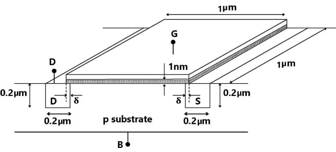
The gate-source overlap capacitance is approximately
Sign in to see the solution
Log in to view the explanation, track your attempts, and keep your progress.
Sign in to UnlockIn the three dimensional view of a silicon n-channel MOS transistor shown below, δ= 20 nm. The transistor is of width 1μm. The depletion width formed at every p-n junction is 10 nm. The relative permittivities of Si and , respectively, are 11.7 and 3.9, and ,= 8.9 x F/m.
The source-body junction capacitance is approximately
Sign in to see the solution
Log in to view the explanation, track your attempts, and keep your progress.
Sign in to UnlockThe channel resistance of an N-channel JFET shown in the figure below is when the full channel thickness of is available for conduction. The built-in voltage of the gate junction is -1 V. When the gate to source voltage is 0 V, the channel is depleted by on each side due to the built-in voltage and hence the thickness available for conduction is only.








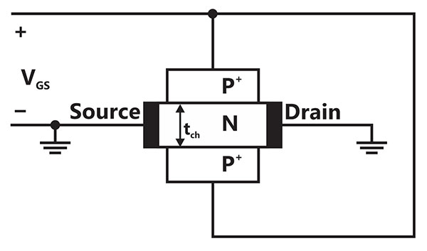
The channel resistance when is




Sign in to see the solution
Log in to view the explanation, track your attempts, and keep your progress.
Sign in to UnlockThe channel resistance of an N-channel JFET shown in the figure below is when the full channel thickness of is available for conduction. The built-in voltage of the gate junction is -1 V. When the gate to source voltage is 0 V, the channel is depleted by on each side due to the built-in voltage and hence the thickness available for conduction is only.
The channel resistance when is




Sign in to see the solution
Log in to view the explanation, track your attempts, and keep your progress.
Sign in to UnlockAt room temperature, a possible value for the mobility of electrons in the inversion layer of a silicon n-channel MOSFET is




Sign in to see the solution
Log in to view the explanation, track your attempts, and keep your progress.
Sign in to UnlockThin gate oxide in a CMOS process in preferably grown using
Sign in to see the solution
Log in to view the explanation, track your attempts, and keep your progress.
Sign in to UnlockConsider the following two statements about the internal conditions in an n-channel MOSFET operating in the active region.
: The inversion charge decreases from source to drain

: The channel potential increases from source to drain

Which of the following is correct?
Only is true.
Both and are false.
Both and are true, but is not a reason for
Both and are true, and is reason for
Sign in to see the solution
Log in to view the explanation, track your attempts, and keep your progress.
Sign in to UnlockThe cross section of a JFET is shown in the following figure. Let be -2V and let be the initial pinch-off voltage. If the width W is doubled (with other geometrical parameters and doping levels remaining the same), then the ratio between the mutual trans-conductance of the initial and the modified JFET is


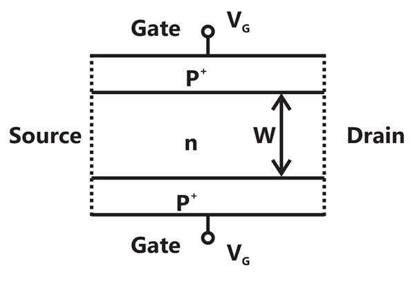
4



Sign in to see the solution
Log in to view the explanation, track your attempts, and keep your progress.
Sign in to UnlockGroup I lists four different semiconductor devices. Match each device in Group I with its characteristic property in Group II.
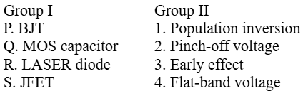
Sign in to see the solution
Log in to view the explanation, track your attempts, and keep your progress.
Sign in to UnlockThe figure shows the high-frequency capacitance-voltage (C-V) characteristics of a Metal//silicon (MOS) capacitor having an area of 1x . Assume that the permittivity of silicon and are 1x F/cm and 3.5x F/cm respectively.



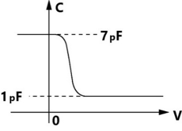
The gate oxide thickness in the MOS capacitor is
Sign in to see the solution
Log in to view the explanation, track your attempts, and keep your progress.
Sign in to UnlockThe figure shows the high-frequency capacitance-voltage (C-V) characteristics of a Metal//silicon (MOS) capacitor having an area of 1x . Assume that the permittivity of silicon and are 1x F/cm and 3.5x F/cm respectively.
The maximum depletion layer width in silicon is
Sign in to see the solution
Log in to view the explanation, track your attempts, and keep your progress.
Sign in to UnlockThe figure shows the high-frequency capacitance-voltage (C-V) characteristics of a Metal//silicon (MOS) capacitor having an area of 1x . Assume that the permittivity of silicon and are 1x F/cm and 3.5x F/cm respectively.
Consider the following statements about the C-V characteristics plot:
: The MOS capacitor has an n-type substrate.
: If positive charges are introduced in the oxide, the C-V plot will shift to the left.
Then which of the following is true?
Both and are true
is true and is false
is false and is true
Both and are false
Sign in to see the solution
Log in to view the explanation, track your attempts, and keep your progress.
Sign in to UnlockA MOS capacitor made using p type substrate is in the accumulation mode. The dominant charge in the channel is due to the presence of
Sign in to see the solution
Log in to view the explanation, track your attempts, and keep your progress.
Sign in to UnlockConsider the following statements and .
: The threshold voltage () of a MOS capacitor decreases with increase in gate oxide thickness

: The threshold voltage () of a MOS capacitor decreases with increase in substrate doping concentration.
Which one of the following is correct?
is FALSE and is TRUE

both and are TRUE

is TRUE and is FALSE
both and are FALSE
Sign in to see the solution
Log in to view the explanation, track your attempts, and keep your progress.
Sign in to UnlockThe drain of an n-channel MOSFET is shorted to the gate so that . The threshold voltage of MOSFET is 1V. If the drain current is 1mA for then for , is





Sign in to see the solution
Log in to view the explanation, track your attempts, and keep your progress.
Sign in to UnlockFor an n-channel enhancement type MOSFET, if the source is connected at a higher potential than that of the bulk (i.e. > 0), the threshold voltage of the MOSFET will

Sign in to see the solution
Log in to view the explanation, track your attempts, and keep your progress.
Sign in to UnlockWhen the gate-to-source voltage of a MOSFET with threshold voltage of 400mV, working in saturation is 900 mV, the drain current in observed to be 1mA. Neglecting the channel width modulation effect and assuming that the MOSFET is operating at saturation, the drain current for an applied of 1400 mV is


Sign in to see the solution
Log in to view the explanation, track your attempts, and keep your progress.
Sign in to UnlockFor a MOS capacitor fabricated on a p-type semiconductor, strong inversion occurs when
Sign in to see the solution
Log in to view the explanation, track your attempts, and keep your progress.
Sign in to UnlockA n-channel silicon MOSFET was fabricated using n + poly-silicon gate and the threshold voltage was found to be 1 V. Now, if the gate is changed to poly-silicon, other things remaining the same, the new threshold voltage should be


Sign in to see the solution
Log in to view the explanation, track your attempts, and keep your progress.
Sign in to UnlockA silicon n MOSFET has a threshold voltage 1 V and oxide thickness of .

[,,]



The region under the gate is ion implemented for threshold voltage tailoring. The dose and type of the implant (assumed to be a sheet charge at the interface) required to shift the threshold voltage to -1V are
, p-type

, n-type
, p-type

, n-type
Sign in to see the solution
Log in to view the explanation, track your attempts, and keep your progress.
Sign in to UnlockThe threshold voltage of an n channel MOSFET can be increased by
Sign in to see the solution
Log in to view the explanation, track your attempts, and keep your progress.
Sign in to UnlockChannel current is reduced on application of a more positive voltage to the gate of a depletion mode n-channel MOSFET. (True=1, False=0)
Sign in to see the solution
Log in to view the explanation, track your attempts, and keep your progress.
Sign in to UnlockAn n-channel JEFT has a pinch-off voltage of, , . The minimum ‘ON’ resistance is achieved in the JEFT for



,


,

,

,
Sign in to see the solution
Log in to view the explanation, track your attempts, and keep your progress.
Sign in to UnlockThe built-in potential of the gate junction of a n-channel JFET is 0.5 volts. The drain current saturates at volts when. The pinch off voltage is __________.


Sign in to see the solution
Log in to view the explanation, track your attempts, and keep your progress.
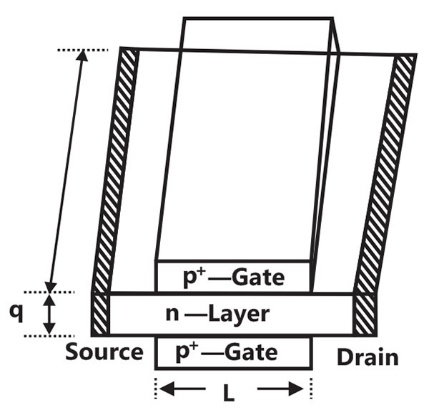
Sign in to UnlockIt is required to use a JFET of figure as linear resistor. The parameters of the JEET are as follows: , , . The doping in the n-layer is and the electron mobility is. The depletion layer width of each junction due to the built in potential is. The two - gate regions are connected together externally. The resistances of the regions outside the gate are negligible. Determine the minimum value of the linear resistor, which can be realized using this JFET without forward biasing the gate junctions.






Sign in to see the solution
Log in to view the explanation, track your attempts, and keep your progress.
Sign in to Unlock