Analog Electronics
OP-AMP and its Applications
Practice questions from OP-AMP and its Applications.
94
Total0
Attempted0
Correct0
IncorrectWhich of the following statements is/are TRUE with respect to an ideal opamp?
Sign in to see the solution
Log in to view the explanation, track your attempts, and keep your progress.
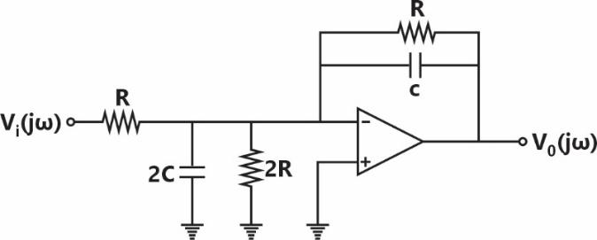
Sign in to UnlockAll the components in the bandpass filter given below are ideal. The lower -3 dB frequency of the filter is 1 MHz.
The upper -3 dB frequency (in MHz, rounded off to the nearest integer) is _________.
Sign in to see the solution
Log in to view the explanation, track your attempts, and keep your progress.
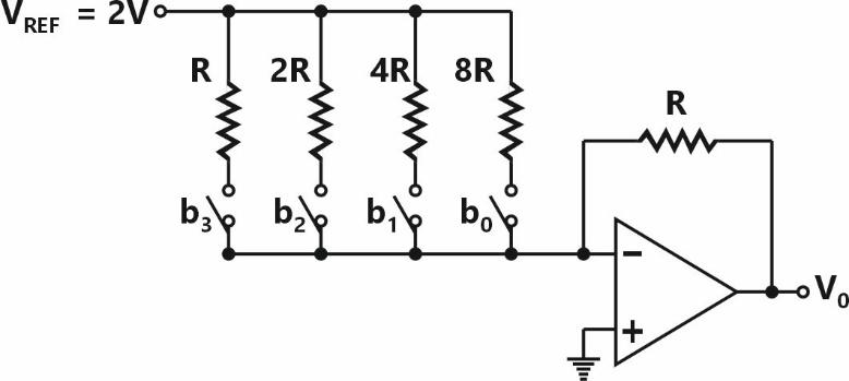
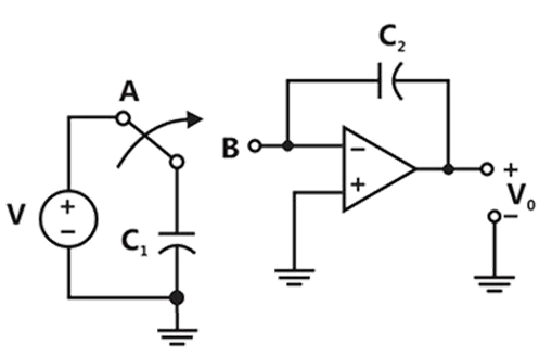
Sign in to UnlockA 4-bit weighted-resistor DAC with inputs , and (MSB to LSB) is designed using an ideal opamp, as shown below. The switches are closed when the corresponding input bits are logic ' 1 ' and open otherwise.


When the input changes from 1110 to 1101, the magnitude of the change in the output voltage , rounded off to the nearest integer) is ___________ .


Sign in to see the solution
Log in to view the explanation, track your attempts, and keep your progress.
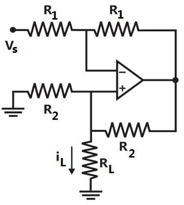
Sign in to UnlockThe opamps in the circuit shown are ideal, but have saturation voltages of .

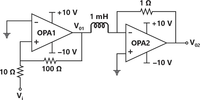
Assume that the initial inductor current is . The input voltage is a triangular signal with peak voltages of and time period of . Which one of the following statements is true?


is delayed by relative to , and is a triangular waveform.


is not delayed relative to , and is a trapezoidal waveform.
is not delayed relative to , and is a triangular waveform.
is delayed by relative to , and is a trapezoidal waveform.

Sign in to see the solution
Log in to view the explanation, track your attempts, and keep your progress.
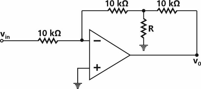
Sign in to UnlockThe of the circuit shown below is


Sign in to see the solution
Log in to view the explanation, track your attempts, and keep your progress.
Sign in to UnlockAn ideal OPAMP circuit with a sinusoidal input is shown in the figure. The frequency is the frequency at which the magnitude of the voltage gain decreases by from the maximum value. Which of the options is/are correct?

The circuit is a low pass filter.
The circuit is a high pass filter
The frequency is .

The frequency is .

Sign in to see the solution
Log in to view the explanation, track your attempts, and keep your progress.
Sign in to UnlockFor the following circuit with an ideal OPAMP, the difference between the maximum and the minimum values of the capacitor voltage is __________


Sign in to see the solution
Log in to view the explanation, track your attempts, and keep your progress.
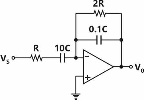
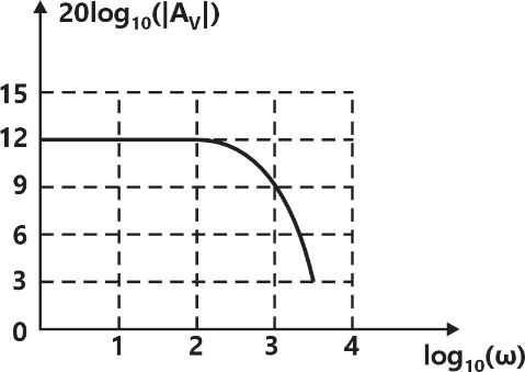
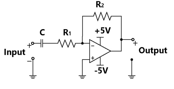
Sign in to UnlockA circuit with an ideal OPAMP is shown. The Bode plot for the magnitude (in ) of the gain transfer function of the circuit is also provided (here, is the angular frequency in . The values of R and are ________.


Sign in to see the solution
Log in to view the explanation, track your attempts, and keep your progress.
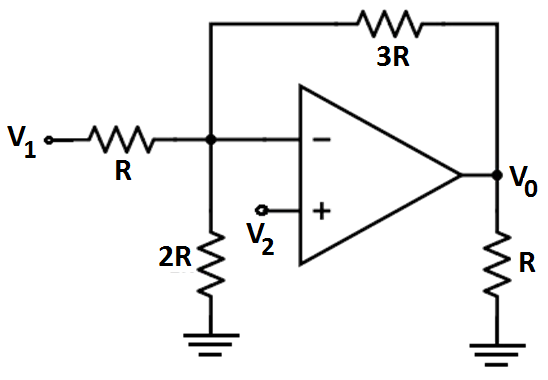
Sign in to UnlockFor the circuit with an ideal Op-Amp shown in the figure, is fixed.

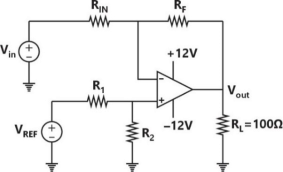
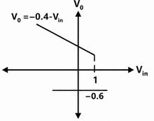
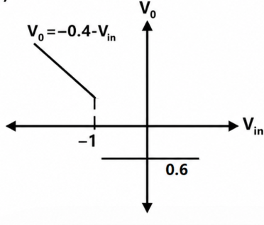
If Volt for Volt and Volt for Volt, where is measured across connected at the output of this Op-Amp, the value of is


Sign in to see the solution
Log in to view the explanation, track your attempts, and keep your progress.
Sign in to UnlockConsider the circuit with an ideal Op-Amp shown in the figure.
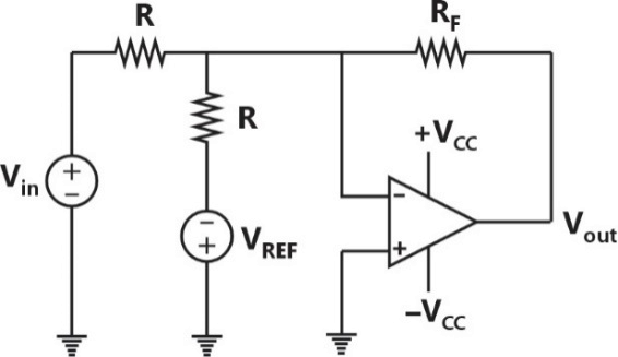
Assuming and , the condition at which equals to zero is


Sign in to see the solution
Log in to view the explanation, track your attempts, and keep your progress.
Sign in to UnlockA circuit with an ideal Op-Amp is shown in the figure. A pulse of duration is applied to the input. The capacitors are initially uncharged.


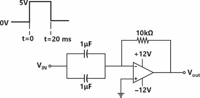
The output voltage of this circuit at (in integer) is ________ V.

Sign in to see the solution
Log in to view the explanation, track your attempts, and keep your progress.
Sign in to UnlockIn the circuit shown below, all the components are ideal. If is , the current sourced by the op-amp is _______ .


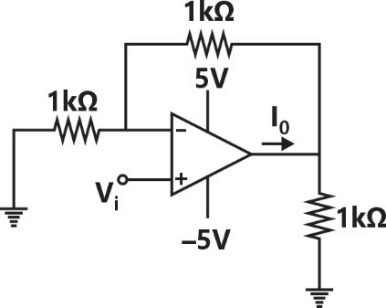
Sign in to see the solution
Log in to view the explanation, track your attempts, and keep your progress.
Sign in to UnlockThe components in the circuit given below are ideal. If and , the cut-off frequency of the circuit in Hz is


Sign in to see the solution
Log in to view the explanation, track your attempts, and keep your progress.
Sign in to UnlockIn the circuit shown below, the op-amp is ideal and Zener voltage of the diode is 2.5 volts. At the input, unit step voltage is applied. i.e.volts. Also, at t =0, the voltage across each of the capacitors is zero.

The time t, in milliseconds, at which the output voltage, crosses -10 V is

Sign in to see the solution
Log in to view the explanation, track your attempts, and keep your progress.
Sign in to UnlockAn op-amp based circuit is implemented as shown below.

In the above circuit, assume the op-amp to be ideal. The voltage (m volts, coned to one decimal place) at node A, connected to the negative input of the op-amp as indicated in the figure is _______
Sign in to see the solution
Log in to view the explanation, track your attempts, and keep your progress.
Sign in to UnlockFor the operational amplifier circuit shown, the output saturation voltages are . The upper and lower threshold voltages for the circuit are, respectively,

Sign in to see the solution
Log in to view the explanation, track your attempts, and keep your progress.
Sign in to UnlockA good transconductance amplifier should have
Sign in to see the solution
Log in to view the explanation, track your attempts, and keep your progress.
Sign in to UnlockThe amplifier circuit shown in the figure is implemented using a compensated operational amplifier (op-amp), and has an open-loop voltage gain, and an open-loop cut-off frequency, . The voltage gain of the amplifier at 15 kHz, in V/V, is _______________ .


Sign in to see the solution
Log in to view the explanation, track your attempts, and keep your progress.
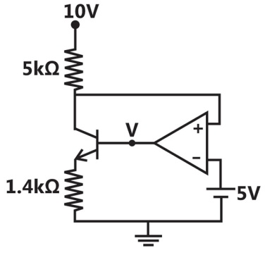
Sign in to UnlockConsider the constant current source shown in the figure below. Let's β represent the current gain of the transistor. The load current through is


Sign in to see the solution
Log in to view the explanation, track your attempts, and keep your progress.
Sign in to UnlockThe following signal of peak voltage 8 V is applied to the non-inverting terminal of an ideal op-amp. The transistor has and .


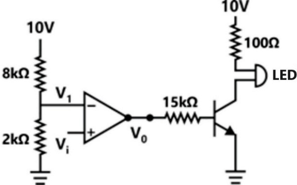
The number of times the LED glows is________________
Sign in to see the solution
Log in to view the explanation, track your attempts, and keep your progress.
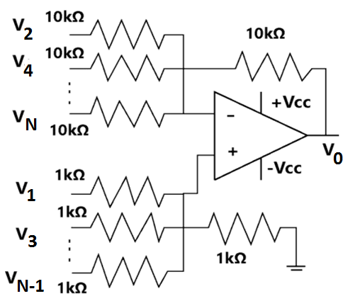
Sign in to UnlockAn ideal op-amp has voltage sources connected to the non-inverting input and connected to the inverting input as shown in the figure below . The voltages ,.... are 1, - 1/2, 1/3, -1/4, 1/5, -1/6,.... volt, respectively. As N approaches infinity, the output voltage (in volt) is_________.


Sign in to see the solution
Log in to view the explanation, track your attempts, and keep your progress.
Sign in to UnlockA PIN photodiode of responsivity 0.8A/W is connected to the inverting input of an ideal op-amp as shown in the figure, Load resistor If 10μW of power is incident on the photodiode, then the value of the photocurrent (in μA) through the load is_______________.


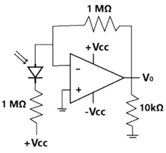
Sign in to see the solution
Log in to view the explanation, track your attempts, and keep your progress.
Sign in to UnlockAn op-amp has a finite open loop voltage gain of 100. Its input offset voltage is modelled as shown in the circuit below. The amplifier is ideal in all other respects. is 25mV.


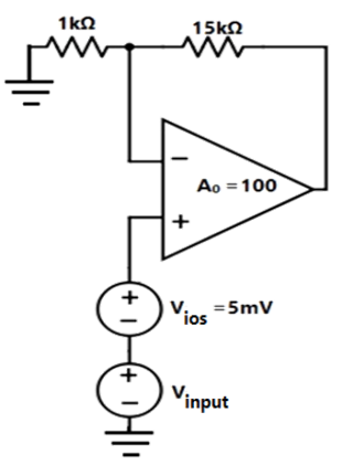
The output voltage (in milli volts) is ________.
Sign in to see the solution
Log in to view the explanation, track your attempts, and keep your progress.
Sign in to UnlockFor the circuit shown in the figure, , L = 1μH and C =1μF. If the input, then the overall voltage gainof the circuit is _________.


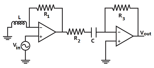
Sign in to see the solution
Log in to view the explanation, track your attempts, and keep your progress.
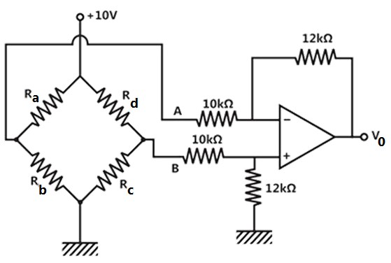
Sign in to UnlockIn the circuit shown, assume that the op-amp is ideal. The bridge output voltage for δ = 0.05 is _______.

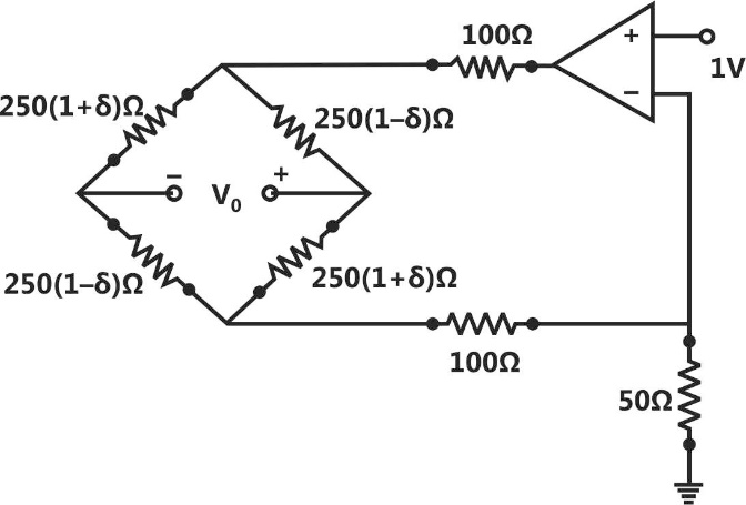
Sign in to see the solution
Log in to view the explanation, track your attempts, and keep your progress.
Sign in to UnlockIn the circuit shown, for switch SW in position A and for SW in position B. Assume that the op-amp is ideal. The value of is ___________.


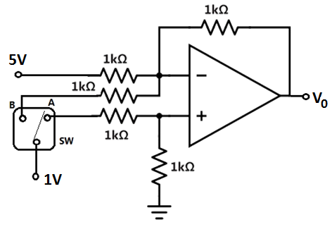
Sign in to see the solution
Log in to view the explanation, track your attempts, and keep your progress.
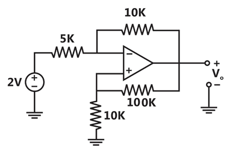
Sign in to UnlockAssuming that the op-amp in the circuit shown below is ideal, the output voltage (in volts) is_______.

Sign in to see the solution
Log in to view the explanation, track your attempts, and keep your progress.
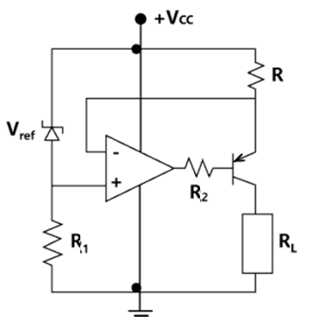
Sign in to UnlockFor the voltage regulator circuit shown, the input voltage is 20 V ± 20% and the regulated output voltage is 10 V. Assume the op-amp to be ideal. For a load drawing 200mA, the maximum power dissipation in (in Watts) is ________.


Sign in to see the solution
Log in to view the explanation, track your attempts, and keep your progress.
Sign in to UnlockIn the circuit shown using an ideal op-amp, the 3-dB cut-off frequency (in Hz) is _______
Sign in to see the solution
Log in to view the explanation, track your attempts, and keep your progress.
Sign in to UnlockIn the circuit shown, assume that the op-amp is ideal. If the gainis –12, the value of R (in kΩ) is _____.

Sign in to see the solution
Log in to view the explanation, track your attempts, and keep your progress.
Sign in to UnlockIn the ac equivalent circuit shown in the figure if is the input current and is very large, the type of feedback is


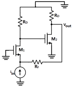
Sign in to see the solution
Log in to view the explanation, track your attempts, and keep your progress.
Sign in to UnlockIn the circuit shown, the op-amp has finite input impedance, infinite voltage gain and zero input offset voltage. The output voltage is

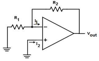


Sign in to see the solution
Log in to view the explanation, track your attempts, and keep your progress.
Sign in to UnlockIn the low-pass filter shown in the figure, for a cut-off frequency of 5kHz, the value of (in kΩ) is _____________.

Sign in to see the solution
Log in to view the explanation, track your attempts, and keep your progress.
Sign in to UnlockIn the voltage regulator circuit shown in the figure, the op-amp is ideal. The BJT has and β = 100, and the zener voltage is 4.7 V. For a regulated output of 9 V, the value of R (in Ω) is _______

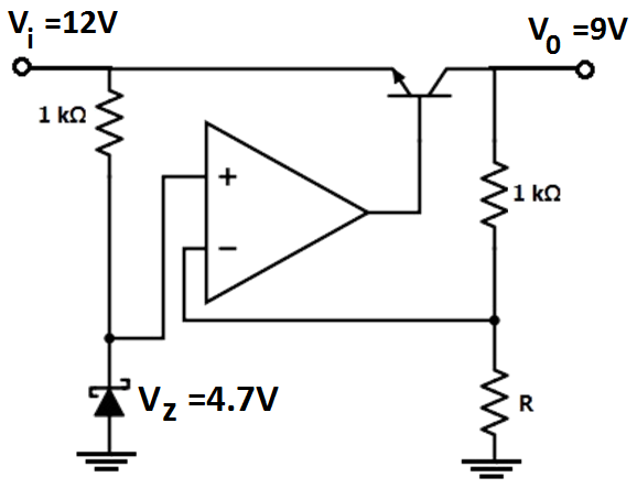
Sign in to see the solution
Log in to view the explanation, track your attempts, and keep your progress.
Sign in to UnlockAssuming that the Op-amp in the circuit shown is ideal, is given by


Sign in to see the solution
Log in to view the explanation, track your attempts, and keep your progress.
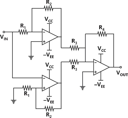
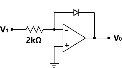
Sign in to UnlockThe circuit shown represents
Sign in to see the solution
Log in to view the explanation, track your attempts, and keep your progress.
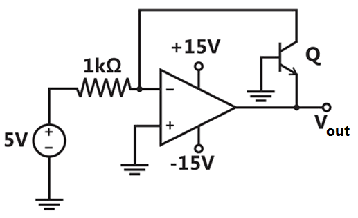
Sign in to UnlockIn the circuit shown below what is the output voltage if a silicon transistor Q and an ideal op-amp are used?

Sign in to see the solution
Log in to view the explanation, track your attempts, and keep your progress.
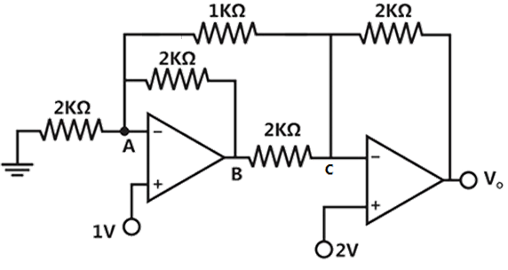
Sign in to UnlockIn the circuit shown below the op-amps are ideal. Then in volts is

Sign in to see the solution
Log in to view the explanation, track your attempts, and keep your progress.
Sign in to UnlockThe circuit shown is a
Low pass filter with

High pass filter with

low pass filter with
High pass filter with
Sign in to see the solution
Log in to view the explanation, track your attempts, and keep your progress.
Sign in to UnlockThe circuit below implements a filter between the input current and the output voltage. Assume that the op-amp is ideal. The filter implemented is a


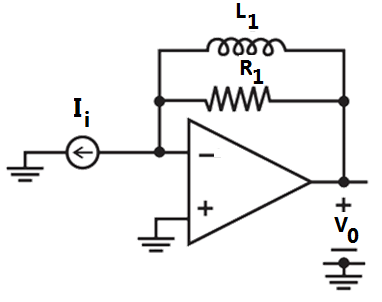
Sign in to see the solution
Log in to view the explanation, track your attempts, and keep your progress.
Sign in to UnlockAssuming the OP-AMP to be ideal, the voltage gain of the amplifier shown below is


Sign in to see the solution
Log in to view the explanation, track your attempts, and keep your progress.
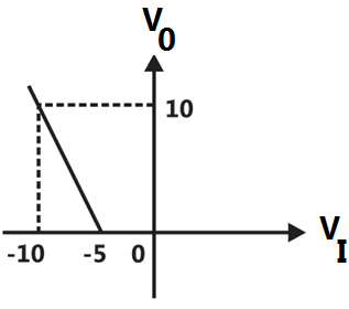
Sign in to UnlockThe transfer characteristic for the precision rectifier circuit shown below is (assume ideal OP-AMP and practical diodes)
Sign in to see the solution
Log in to view the explanation, track your attempts, and keep your progress.
Sign in to UnlockIn the circuit shown below, the op-amp is ideal, the transistor has and . Decide whether the feedback in the circuit is positive or negative and determine the voltage V at the output of the op-amp.


Sign in to see the solution
Log in to view the explanation, track your attempts, and keep your progress.
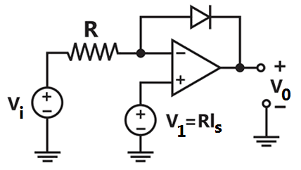
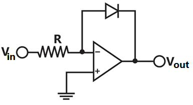
Sign in to UnlockConsider the following circuit using an ideal OPAMP. The I-V characteristics of the diode is described by the relation where, and V is the voltage across the diode (taken as positive for forward bias). For an input voltage, the output voltage is


Sign in to see the solution
Log in to view the explanation, track your attempts, and keep your progress.
Sign in to UnlockThe OPAMP circuit shown above represents a
Sign in to see the solution
Log in to view the explanation, track your attempts, and keep your progress.
Sign in to UnlockFor the Op-Amp circuit shown in the figure, , is

Sign in to see the solution
Log in to view the explanation, track your attempts, and keep your progress.
Sign in to UnlockIn the Op-Amp circuit shown, assume that the diode current follows the equation . For , and for The relationship between and is


Sign in to see the solution
Log in to view the explanation, track your attempts, and keep your progress.
Sign in to UnlockConsider the Op-Amp circuit shown in the figure.
The transfer function is


Sign in to see the solution
Log in to view the explanation, track your attempts, and keep your progress.
Sign in to Unlockand, then the minimum and maximum values of (in radians) are respectively


Sign in to see the solution
Log in to view the explanation, track your attempts, and keep your progress.
Sign in to UnlockFor the circuit shown in the following figure, the capacitor C is initially uncharged. At t = 0, the switch S is closed. The voltage across the capacitor at

t = 1 millisecond is:
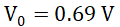
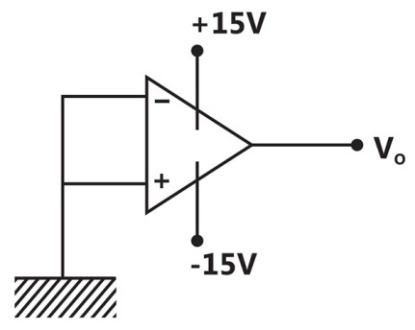
In the figure shown, the OP-AMP is supplied with and the ground has been shown by the symbol


Sign in to see the solution
Log in to view the explanation, track your attempts, and keep your progress.
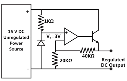
Sign in to UnlockA regulated power supply, shown in figure below, has an unregulated input (UR) of 15 Volts and generates a regulated output. Use the component values shown in the figure.
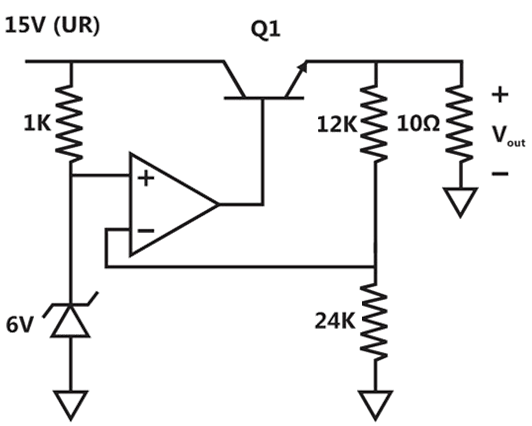
In the figure above, the ground has been shown by the symbol
The power dissipation across the transistor shown in the figure is:
Sign in to see the solution
Log in to view the explanation, track your attempts, and keep your progress.
Sign in to UnlockA regulated power supply, shown in figure below, has an unregulated input (UR) of 15 Volts and generates a regulated output. Use the component values shown in the figure.
In the figure above, the ground has been shown by the symbol
If the unregulated voltage increases by 20%, the power dissipation across the transistor
Sign in to see the solution
Log in to view the explanation, track your attempts, and keep your progress.
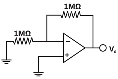
Sign in to UnlockThe input resistance of the amplifier shown in figure is

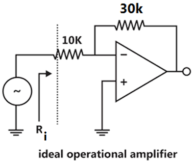


infinite
Sign in to see the solution
Log in to view the explanation, track your attempts, and keep your progress.
Sign in to UnlockThe voltage indicated in figure has been measured by an ideal voltmeter. Which of the following can be calculated?

Sign in to see the solution
Log in to view the explanation, track your attempts, and keep your progress.
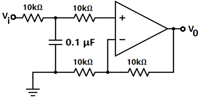
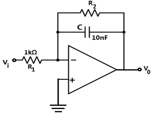
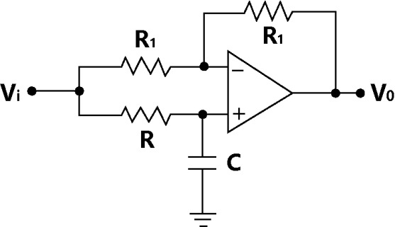
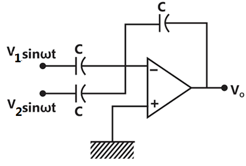
Sign in to UnlockThe op-amp circuit shown in figure is a filter. The type of filter and its cut-off frequency are respectively.
Sign in to see the solution
Log in to view the explanation, track your attempts, and keep your progress.
Sign in to UnlockAn ideal op-amp is an ideal
Sign in to see the solution
Log in to view the explanation, track your attempts, and keep your progress.
Sign in to UnlockThe circuit in the figure is a
Sign in to see the solution
Log in to view the explanation, track your attempts, and keep your progress.
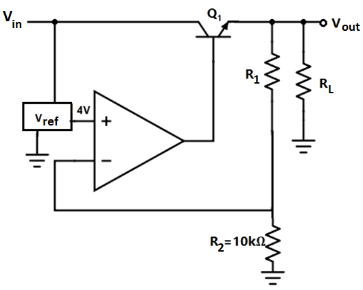
Sign in to UnlockIn the op-amp circuit given in Figure, the load current is


Sign in to see the solution
Log in to view the explanation, track your attempts, and keep your progress.
Sign in to UnlockIf the input to the ideal comparator shown in figure is a sinusoidal signal of 8V (peak to peak) without any DC component, then the output of the comparator has a duty cycle of


Sign in to see the solution
Log in to view the explanation, track your attempts, and keep your progress.
Sign in to UnlockThe output voltage of the regulated power supply shown in figure is
Sign in to see the solution
Log in to view the explanation, track your attempts, and keep your progress.
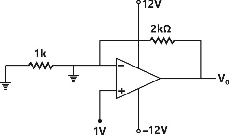
Sign in to UnlockIf the op-amp in the figure is ideal, the output voltage will be equal to
Sign in to see the solution
Log in to view the explanation, track your attempts, and keep your progress.
Sign in to UnlockA 741-type op-amp has a gain-bandwidth product of 1MHz. A non-inverting amplifier using this op-amp and having a voltage gain of 20dB will exhibit a 3-dB bandwidth of
50 KHz
100 KHz


Sign in to see the solution
Log in to view the explanation, track your attempts, and keep your progress.
Sign in to UnlockAn amplifier using an op-amp with a slew-rate
SR = 1V/μsec has a gain of 40dB. If this amplifier has to faithfully amplify sinusoidal signals from dc to 20KHz without introducing any slew-rate induced distortion, then the input signal level must not exceed.
Sign in to see the solution
Log in to view the explanation, track your attempts, and keep your progress.
Sign in to UnlockConsider the circuit of Figure. The op-amp used is ideal.
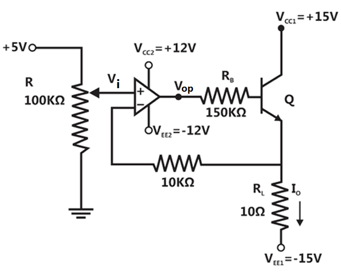
(a) In which mode is the BJT operating (i.e. active, saturation or cut-off)? Justify your answer.
(b) Obtain an expression relating the output current and the input voltage.


(c) Determine and if volt ( : output of OP-AMP)


(Assume β = 99 and )

(a) Active Region
(a) Saturation
(b)

(c) and


Sign in to see the solution
Log in to view the explanation, track your attempts, and keep your progress.
Sign in to UnlockThe ideal OP-AMP has the following characteristics.


Sign in to see the solution
Log in to view the explanation, track your attempts, and keep your progress.
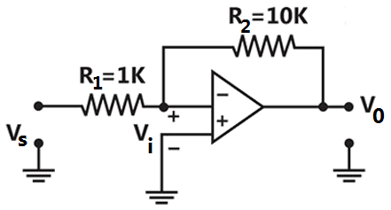
Sign in to UnlockThe inverting OP-AMP shown in Figure has an open-loop gain of 100. The closed loop gain is

Sign in to see the solution
Log in to view the explanation, track your attempts, and keep your progress.
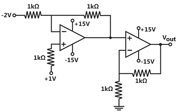
Sign in to UnlockIn Figure, assume the OP-AMPs to be ideal. The output of the circuit is:

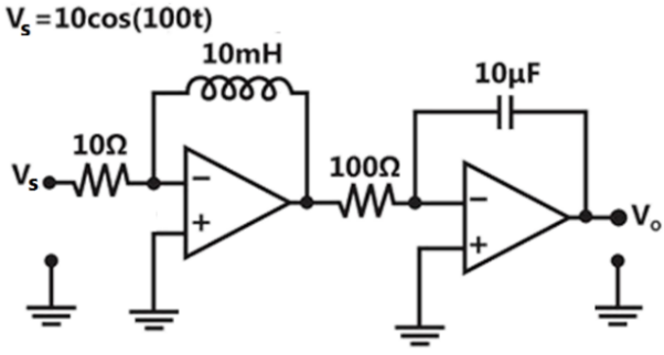
10 cos (100t)


Sign in to see the solution
Log in to view the explanation, track your attempts, and keep your progress.
Sign in to UnlockAssume that the OP-AMP in Figure is ideal.
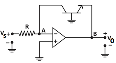
(a) Obtain an expression for in terms of, R, and the reverse saturation current of the transistor.


(b) If R = 1Ω, and the thermal voltage, then what is the value of the output voltage for an input voltage ?


(c) Suppose that the transistor in the feedback path is replaced by a p-n-junction diode with a reverse saturation current of The p-side of the diode is connected to node A and the n-side to node B. Then what is the expression for in terms of, R, ?


(a)

(b)

(c)

(b)
Sign in to see the solution
Log in to view the explanation, track your attempts, and keep your progress.
Sign in to UnlockIn the circuit of Figure, is

Sign in to see the solution
Log in to view the explanation, track your attempts, and keep your progress.
Sign in to UnlockIf the op-amp in Figure, is ideal then, is
Zero


Sign in to see the solution
Log in to view the explanation, track your attempts, and keep your progress.
Sign in to UnlockAssume that the op-amp of Figure is ideal. If is a triangular wave, then will be

Sign in to see the solution
Log in to view the explanation, track your attempts, and keep your progress.
Sign in to UnlockThe most commonly used amplifier in sample and hold circuits is
Sign in to see the solution
Log in to view the explanation, track your attempts, and keep your progress.
Sign in to UnlockIf the OP-AMP in the figure has an input offset voltage of 5mV and an open-loop voltage gain of 10,000, then will be
Sign in to see the solution
Log in to view the explanation, track your attempts, and keep your progress.
Sign in to UnlockThe first dominant pole encountered in the frequency response of a compensated op-amp is approximately at
Sign in to see the solution
Log in to view the explanation, track your attempts, and keep your progress.
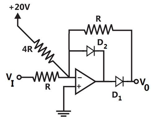
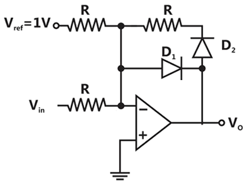
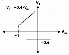
Sign in to UnlockNeatly sketch and label the dc transfer characteristic (i.e. ) of the circuit shown in Figure, as varies from -2V to +2V. Assume ideal op-amp, and the diodes have a forward voltage of 0.6 V and zero incremental resistance.


Sign in to see the solution
Log in to view the explanation, track your attempts, and keep your progress.
Sign in to UnlockOne input terminal of high gain comparator circuit is connected to ground and a sinusoidal voltage is applied to the other input. The output of comparator will be
Sign in to see the solution
Log in to view the explanation, track your attempts, and keep your progress.
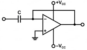
Sign in to UnlockDetermine the input impedance of the circuit of the figure and investigate if it can be inductive.
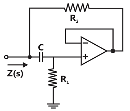
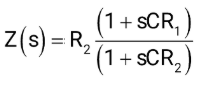
this circuit can act as an inductor
this circuit cannot act as an inductor
Sign in to see the solution
Log in to view the explanation, track your attempts, and keep your progress.
Sign in to UnlockThe output voltage of the circuit shown in the figure is

Sign in to see the solution
Log in to view the explanation, track your attempts, and keep your progress.
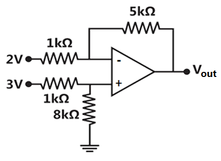
Sign in to UnlockConsider the circuit given in the figure is using an ideal operational amplifier.
The characteristics of the diode are given by the relation

Where is the forward voltage across the diode

(a) Express as function of assuming

(b) If, and , find the input voltage for which


(a)

(b)

(b)
None of these
Sign in to see the solution
Log in to view the explanation, track your attempts, and keep your progress.
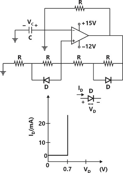
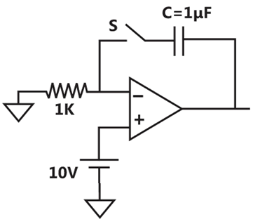
Sign in to UnlockIn the circuit shown in the figure is assume that the operational amplifier is ideal and that initially. The switch is connected first to ‘A’ charging to the voltage V. It is then connected to the point ‘B’. This process is repeated f times per second.


(a) Calculate the charge transferred per second from node A to node B.
(b) Derive the average rate of change of the output voltage.
(c) If the capacitor and the switch are removed and a resistor is connected between points A and B, find the value of the resistor to get the same average rate of change of the output voltage?
(d) If the repetition rate of the switching action is times per second, , and , what is the average rate of change of the output voltage?


(a) Charge transferred per second from node A to node B

(b) Average rate of charge

(c)

(d) Average rate of change of the output voltage

Sign in to see the solution
Log in to view the explanation, track your attempts, and keep your progress.
Sign in to UnlockThe circuit shown in the figure is that of
Sign in to see the solution
Log in to view the explanation, track your attempts, and keep your progress.
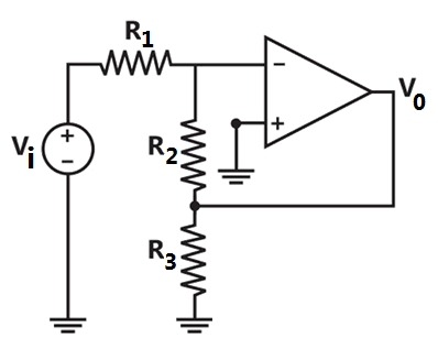
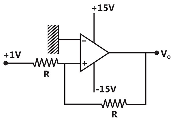
Sign in to UnlockIn the given circuit the given figure, if the voltage inputs and are to be amplified by the same amplification factor, the value of R should be


Sign in to see the solution
Log in to view the explanation, track your attempts, and keep your progress.
Sign in to UnlockAn OP-AMP is used as a zero-crossing detector. If the maximum output available from the OP-AMP is p-p, and the slew rate of the OP-AMP is , then the maximum frequency of the input signal that can be applied without causing a reduction in the p-p output is ______________kHz.


Sign in to see the solution
Log in to view the explanation, track your attempts, and keep your progress.
Sign in to UnlockThe frequency compensation is used in op-amps to increase its stability. ( True=1, False=0)
Sign in to see the solution
Log in to view the explanation, track your attempts, and keep your progress.
Sign in to UnlockFor the ideal op-amp circuit of figure shown, determine the outpout voltage ______V

Sign in to see the solution
Log in to view the explanation, track your attempts, and keep your progress.
Sign in to UnlockFind the output, (V) in the following circuit (figure), assuming that the op-amps are ideal.
Sign in to see the solution
Log in to view the explanation, track your attempts, and keep your progress.
Sign in to UnlockAn op-amp has an offset voltage of 1mV and is ideal in all other respects. If this op-amp is used in the circuit shown in figure, the output voltage will be (select the nearest value)
1 mV
1 V

0 V
Sign in to see the solution
Log in to view the explanation, track your attempts, and keep your progress.
Sign in to UnlockThe circuit of figure, uses an ideal op amp. For small positive values of , the circuit works as
Sign in to see the solution
Log in to view the explanation, track your attempts, and keep your progress.
Sign in to UnlockAssume that the operational amplifier in figure is ideal. The current I, through the 1K ohm resistor is __________mA.
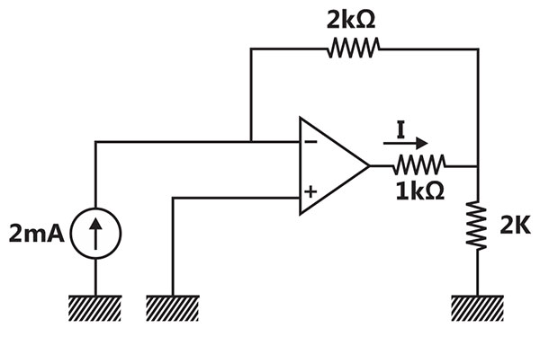
Sign in to see the solution
Log in to view the explanation, track your attempts, and keep your progress.
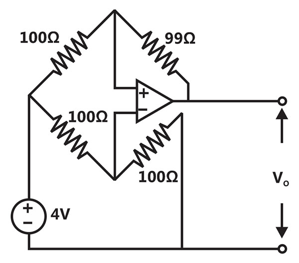
Sign in to UnlockConsider the circuit shown in the figure. This circuit uses an ideal operational amplifier. Assuming that the impedances at nodes A and B do not load the preceding bridge circuit; calculate the output voltage

(a) When ohms

(b) When ohms and ohms


(a)

(b)

(a)
(b)
Sign in to see the solution
Log in to view the explanation, track your attempts, and keep your progress.
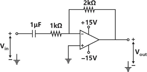
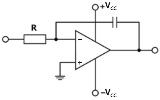
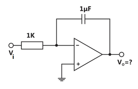
Sign in to UnlockIn order that the circuit of Figure works properly as differentiator, it should be modified to ____________ (draw the modified circuit)
Sign in to see the solution
Log in to view the explanation, track your attempts, and keep your progress.
Sign in to UnlockTwo non-inverting amplifiers, one having a unity gain and the other having a gain of twenty are made using identical operational amplifiers. As compared to the unity gain amplifier, the amplifier with gain twenty has
Sign in to see the solution
Log in to view the explanation, track your attempts, and keep your progress.
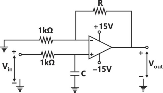
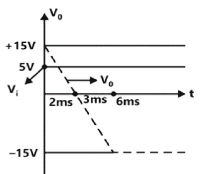
Sign in to UnlockIn figure, the operational amplifier is ideal and its output can swing between -15 and +15 volts. The input which is zero for , is switched to 5 volts at the instant . Given that the output is +15 volts for , sketch on the same diagram the waveforms of and . You must give the values of important parameters of this sketch.


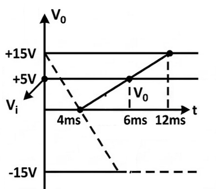
Sign in to see the solution
Log in to view the explanation, track your attempts, and keep your progress.
Sign in to UnlockIn figure, the operational amplifiers are ideal and their output can swing between -15 and +15 volts. Sketch on same diagram the waveform of voltages and as a function of time. You must give the values of important parameters of this sketch.


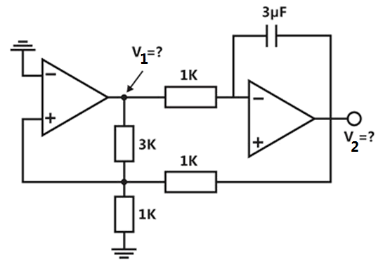
For


For


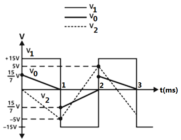
None of these
Sign in to see the solution
Log in to view the explanation, track your attempts, and keep your progress.
Sign in to Unlock